VT82C42 データシートの表示(PDF) - Unspecified
部品番号
コンポーネント説明
一致するリスト
VT82C42 Datasheet PDF : 13 Pages
| |||
VIA Technologies, Inc.
VT82C42
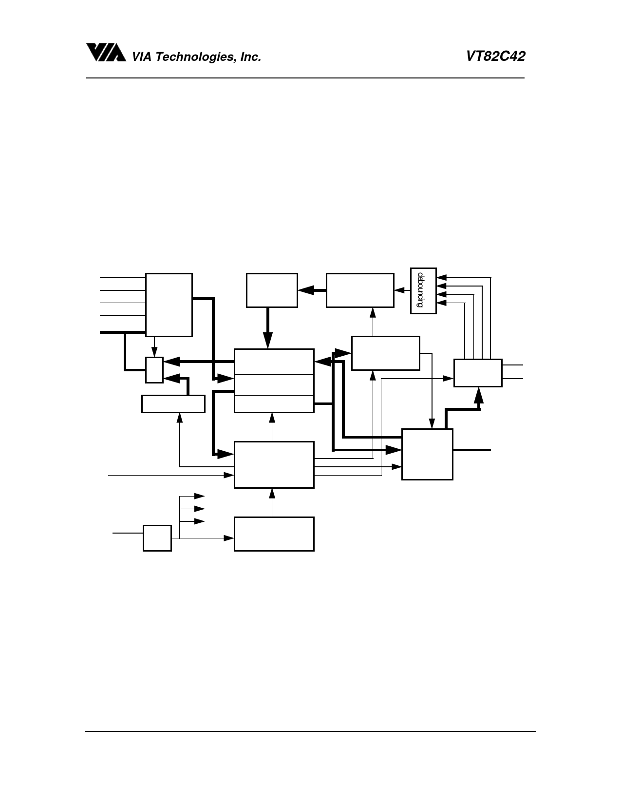
The host can program the output port (P20-P23 in AT mode, or P20-P21 in PS/2 mode) or in-out port (P10-
P15 in AT mode, or P12-P15 in PS/2 mode) by issuing a command to the command register on the VT82C42.
The controller will then quickly execute the specified command. Note that P16-P17 is implemented as an
input port only. The host can also transmit data to the keyboard and mouse by issuing a command to the data
register. The data coming to the data register (with A0 = 0, CS# = 0, RD# = 1, and WR# = 0) will be sent to
the keyboard via the keyboard serial interfaces. The data sent to the mouse will be completed by 1) issuing a
D4 command to the command register, 2) then writing the following data byte to the data register (to be sent to
the mouse via mouse serial interface). In either case, the VT82C42 will wait for an acknowledgement from the
keyboard or mouse to complete a transmission. At the same time as the completion of the transmission, the
VT82C42 will raise P24 or P25 (when sending data to mouse) to signal the host of a completion of
transmission. When the controller receives or transmits, the controller does a parity and time-out check. If any
error occurs in the interface or inside the external devices (keyboard or mouse), the controller will reflect that
error in the following status register.
A0
CS
IOR
command
IOW
decoder
scan
mapping
receiving unit
KBCK
KBDT
MSCK
MSDT
D[7:0]
+
status register
datainput buffer
commandregister/
dataregister
dataoutput buffer
transmitting unit
T1
mode
selector
T0
RESET
arbitration &
central control
unit
In/Out
port buffer
P[17:10]
P[27:20]
X1, X2
clocking
(8 Mhz)
timer
Fig 1. Block Diagram for VT82C42
-2-
Share Link: 