VT82885 データシートの表示(PDF) - Unspecified
部品番号
コンポーネント説明
一致するリスト
VT82885 Datasheet PDF : 16 Pages
| |||
VIA Technologies, Inc.
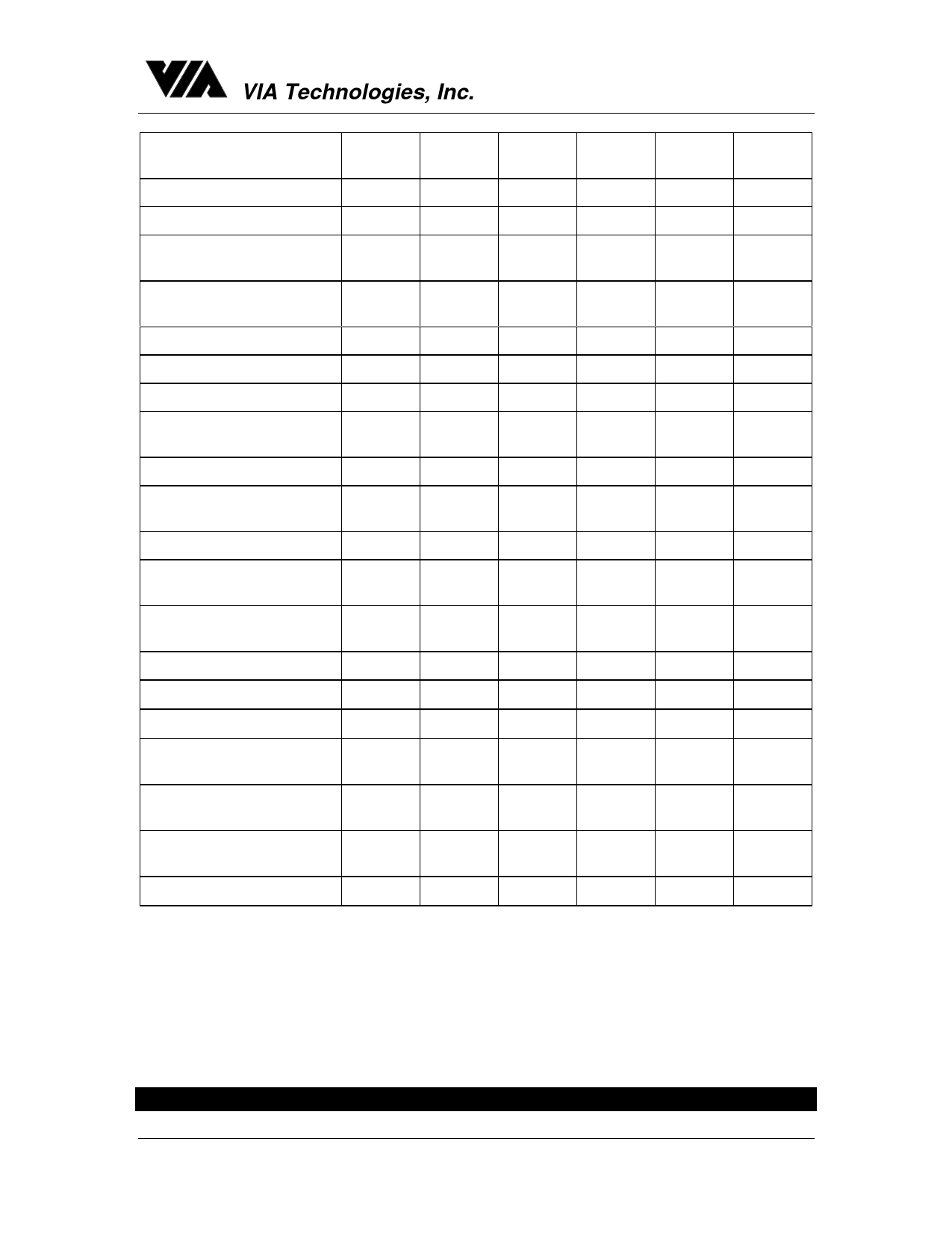
Pulse Width, DS/E High or PWEH
125
RD/WR# Low
Input Rise and Fall Time
tR, tF
R/W# Hold Time
tRWH
10
R/W# Setup Time
before DS/E
tRWS
50
Chip Select Setup Time
tCS
20
before DS, WR#, or RD#
Chip Select Hold Time
tCH
0
Read Data Hold Time
tDHR
10
Write Data Hold Time
tDHW
0
Muxed Address Valid Time tASL
30
to AS/ALE Fall
Muxed Address Hold Time tAHL
10
Delay Time DS/E
to AS/ALE Rise
tASD
25
Pulse Width AS/ALE High PWASH
60
Delay Time, AS/alE
to DS/E Rise
tASED
40
Output Data Delay Time
tDDR
20
from DS/E or RD#
DataSetup Time
Reset Pulse Width
IRQ# Release from DS
IRQ# Release from
RESET#
tDSW
100
tRWL
5
tIRDS
tIRR
Delay Time before Update
Cycle
tBUC
Periodic Interrupt Time
tPI
Interval
Time of Update Cycle
tUC
244
1708
VT82885
Real Time Clock
ns
30
ns
ns
ns
ns
ns
80
ns
ns
ns
ns
ns
ns
120
ns
ns
µs
2
µs
2
µs
µs
See Table
1
µs
NOTES
1. All voltages are referenced to ground.
2. All outputs are open.
3. Applies to the AD0-AD7 pins, the IRQ#
FIGURE 4: OUTPUT LOAD
pin and the SQW pin when each is in the
high impedence state.
4. The IRQ# pin is open drain.
5. Measured with a load as shown in
Figure 4.
12
Share Link: 