UPD7759C データシートの表示(PDF) - NEC => Renesas Technology
部品番号
コンポーネント説明
一致するリスト
UPD7759C Datasheet PDF : 18 Pages
| |||
µPD7759
1. PIN FUNCTIONS
5
1.1 COMMON FUNCTION TO ALL MODES
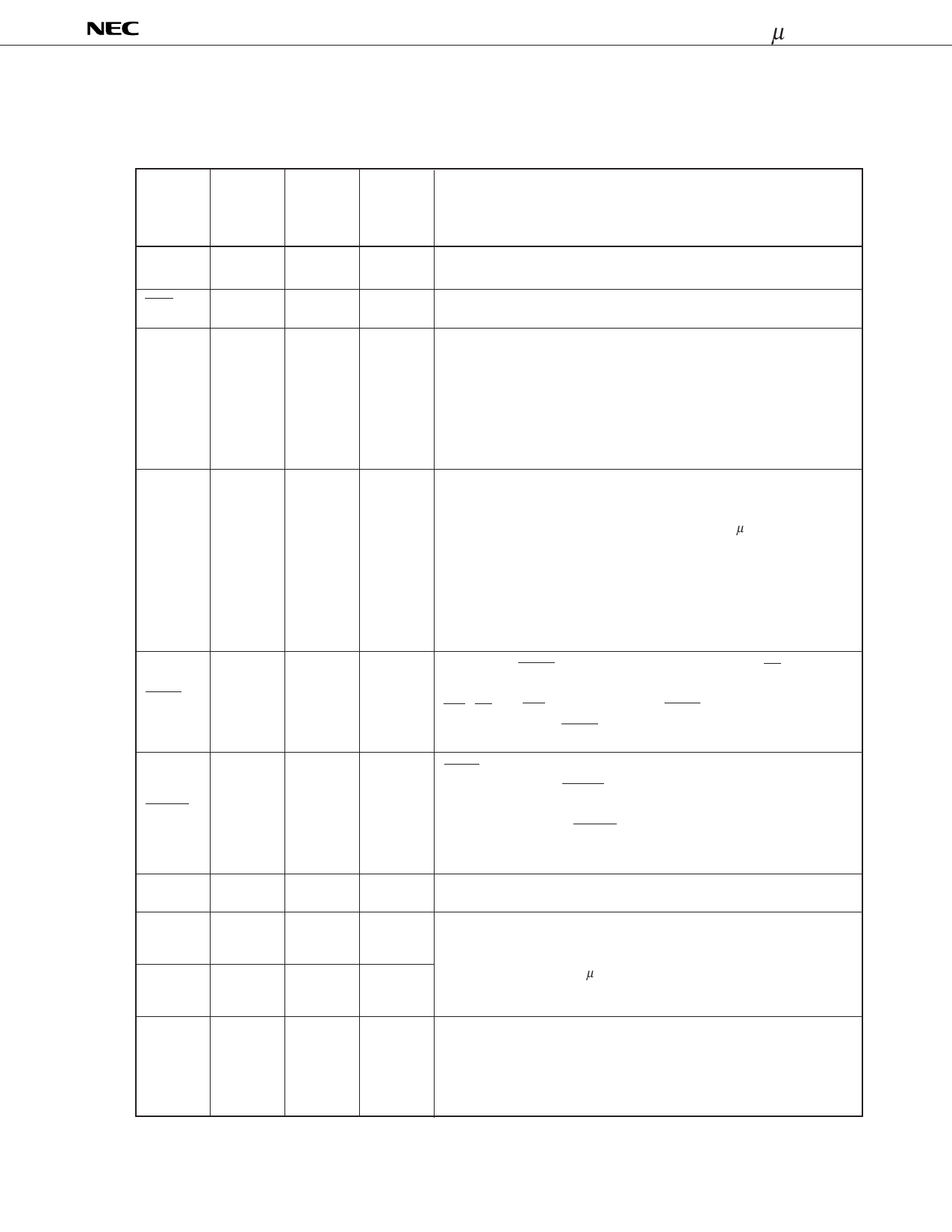
Pin
52-pin
40-pin
(Abbre-
QFP
DIP
I/O
viation) Pin No. Pin No.
Function
VDD
DRQ
6
40
—
Power supply (2.7 to 5.5 V)
24
14
Output Speech synthesis data request.
D/A converter reference current input.
The sink-load current input causes the output current of the
D/A converter to change.
REF
28
16
Input
The D/A converter reference current is passed to VDD via
a resistor.
In standby mode, REF is set to high impedance.
AVO
Analog speech signal output.
AVO outputs a unipolar sink-load current.
The output current is reduced to 0 when the µPD7759 is in the
standby mode.
29
17
Output
The output current of the D/A converter from AVO is changed
according to the input current from REF.
Maximum output current of the D/A converter is approx. the
34 times the REF input current.
Active-low BUSY signal output. When inputting ST signal,
it outputs a low level signal.
BUSY
30
18
Output
MD, ST and WR are invalid while BUSY is low.
In standby mode, BUSY is set to high impedance.
RESET
31
Reset input.
In standby mode, RESET must be at low level more than 12
19
Input clock cycles after clock oscillation becomes stable.
In operation mode, RESET must be at low level for 12 clock
cycles (oscillation clock).
GND
32
20
—
Ground.
X1
36
23
—
Ceramic resonator connection for generating a clock signal.
The 640 kHz ceramic resonator can be connected.
In standby mode, the µPD7759 outputs a low-level to X1 and
X2
37
24
—
a high-level to X2.
1, 7, 13,
14, 20, 26,
NC
—
27, 33, 39,
40, 46, 52
—
No Connection
3
Share Link: 