UPD161660 データシートの表示(PDF) - NEC => Renesas Technology
部品番号
コンポーネント説明
一致するリスト
UPD161660 Datasheet PDF : 15 Pages
| |||
µPD161660
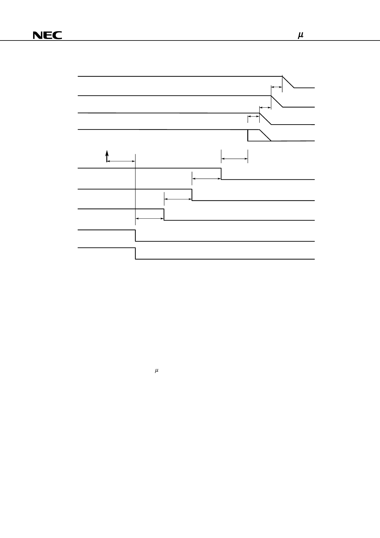
5.2 Power OFF sequence
VDC
VCC1
VCC2
/RESET
DCON
RGONP
RGONG
OE1
OE2
0 ns
0 ns
0 ns
STBY
command
< 1-frame
tRPDD
0 ns
tOE2RG
tRGRP
Remark OE1, OE2, /RESET, RGONG, RGONP, VCC2 are the signals from driver.
x Input the STBY command (↑part).
The source driver sets the status of the OE1 and OE2 pins to low level within one frame.
The gate output is fixed to VT.
y Set a timing that ensures the RGONG, RGONP, and DCON pins are shifted to low level in that order after the
panel load has been sufficiently discharged (tOE2RG timing; Secure an amount of time equivalent to one frame after
executing the standby command). At this time, the DC/DC converter and the regulators are off.
Note that a timing of 0 ns for tRGRP and tRPDD causes no problems on the device side, but users are requested to set
the final timing after sufficiently evaluating the µPD161660 in the LCD module.
z Although it is unnecessary to input the RESET command to the source driver, for designs in which the system is
reset when the power supply is turned off, make settings that ensure /RESET = L at DCON = L and subsequent
timings.
{ All three power supplies, VDC, VCC1, and VCC2, can be off at the same time.
12
Data Sheet S14799EJ1V0DS
Share Link: 