UPD161644P データシートの表示(PDF) - NEC => Renesas Technology
部品番号
コンポーネント説明
一致するリスト
UPD161644P Datasheet PDF : 51 Pages
| |||
µPD161644
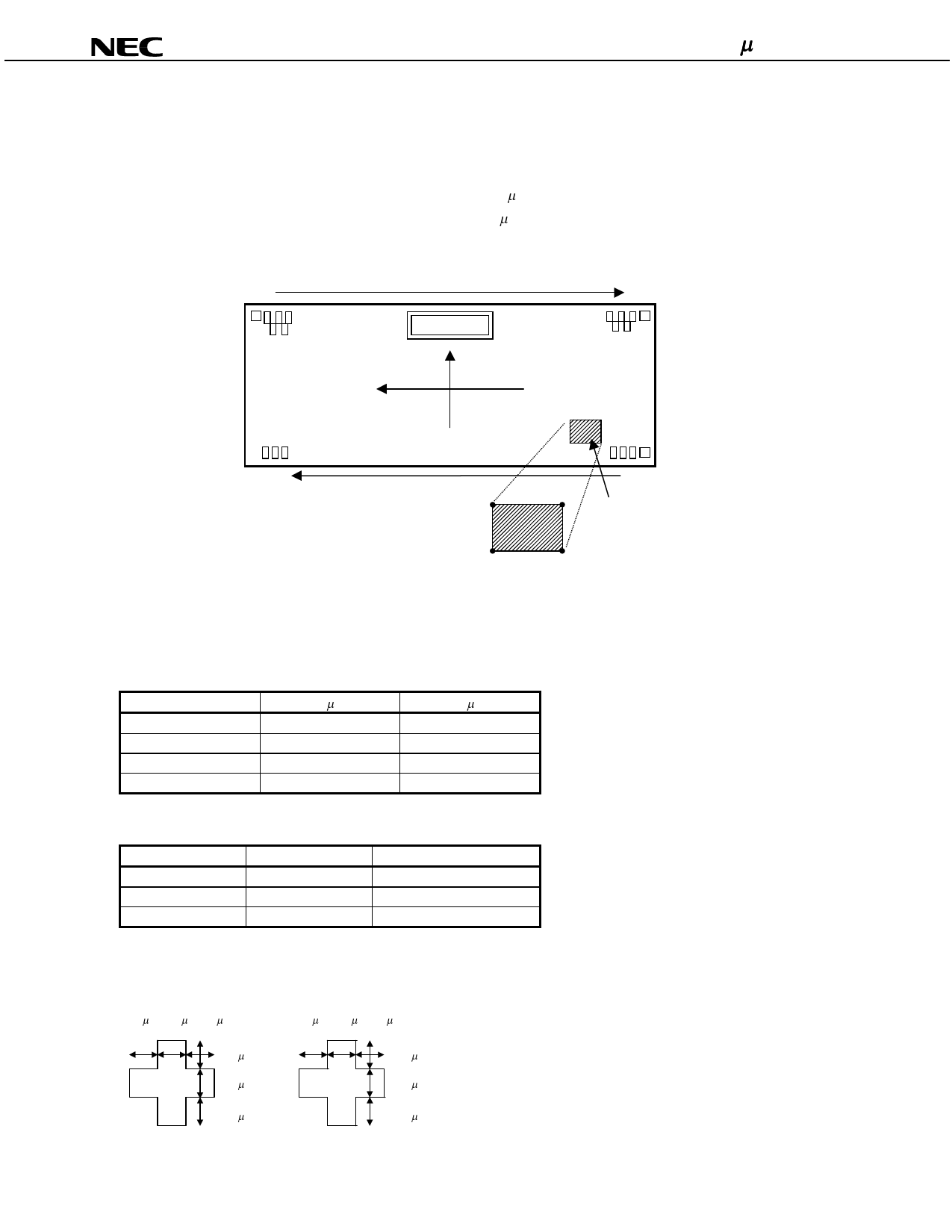
2. PIN CONFIGURATION (Pad Layout)
Chip size: 2.8 x 9.4 mm2
Bump size
Input/Left/Right (includes DUMMY of input side)
Output (includes DUMMY output side)
: 100 x 40 µm2
: 86 x 35 µm2
No.145
+
Figure 2-1. Chip Schematic
Bump side up
X
Y
(0,0)
No.391
+
No.144
+
No.1
A
B
Note
Opening in protective film
C
D
Note A part of the protective film on the chip surface is absent to enable a transistor check at shipment.
The position of this opening is indicated by the shaded section in the above chip schematic. The specific
coordinates of this opening are as follows.
X (µm)
Y (µm)
A
−847.74
−3143.37
B
−687.75
−3143.37
C
−687.75
−3438.78
D
−847.74
−3438.78
Alignment Mark Coordinate (mark center, unit: mm)
X
−1.125
0.9705
0.9705
Y
−4.5705
4.5495
−4.5495
Shape of Alignment Mark
Type A
Type B
Type B
Alignment Mark
Type A
10 µm 10 µm 10 µm
10 µm
10 µm
10 µm
Type B
30 µm 30 µm 30 µm
30 µm
30 µm
30 µm
6
Preliminary Product Information S15797EJ1V4PM
Share Link: 