UPD161644 データシートの表示(PDF) - NEC => Renesas Technology
部品番号
コンポーネント説明
一致するリスト
UPD161644 Datasheet PDF : 51 Pages
| |||
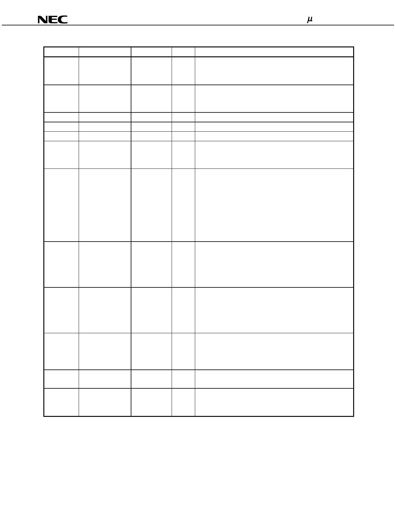
µPD161644
Symbol
VS
MVS
Pin Name
Positive power
output supply for
driver
External resistor
input
Pad No.
118 to 123
117
PVCC1
PVSS1
PVSS3
CLK
Pull-up voltage
Pull-down voltage
Pull-down voltage
Shift clock input
6, 24, 125
20, 27, 131
21
139
STVR,
STVL
Start pulse
136,
input/output pin
137
OE1
Enable input
140
OE2
Enable input
141
R,/L
Shift direction
25
control
FRM
DCCLK
Frame signal input 129
Clock input for
138
DC/DC converter
(2/5)
I/O
Function
Output Positive power supply voltage output for source driver. The VS
output voltage can be changed by setting VSEL0 to VSEL2.
Input
−
−
−
Input
I/O
Input
Input
Input
Input
Input
Any output voltage can be set by connecting an external resistor.
<EXRV = 0> Leave open.
<EXRV = 1> Connect to external resistor.
Pull-up voltage for mode setting pin.
Pull-down voltage for mode setting pin.
Pull-down voltage for mode setting pin.
Shift clock input pin of the internal shift resistor. The contents of
internal shift resistor are shifted at the rising edge of CLK.
Connect to GCLK pin of source driver.
Input/output pin of the internal shift resistor.
Start pulse signal is read at the rising edge of shift clock CLK and a
scan signal is output from the driver output pin.
The valid level of the STVR/STVL pin is determined by the setting
of STVSEL.
When STVSEL = L, the pulse becomes low level at the falling
edge of the 240th shift clock CLK and high level at falling edge of
the 241st clock.
If the level selected by OE1SEL is input, the driver output is fixed to
low level (When OE1SEL = L the driver output is fixed to low level if
a low level is input). However, the shift resistor is not cleared. And,
output enable actuation is asynchronous in the clock.
Connect to GOE1 pin of source driver.
If the level selected by OE2SEL is input, the driver output is fixed to
high level (When OE2SEL = L the driver output is fixed to low level
if a high level is input). However, the shift resistor is not cleared.
And, output enable actuation is asynchronous in the clock.
Connect to GOE2 pin of source driver.
The shift direction control pin of shift register. The shift directions
of the shift registers are as follows.
R,/L = H (right shift): STVR input, O1 →O241, STVL output
R,/L = L (left shift) : STVL input, O241 → O1, STVR output
Input frame reverse signals.
Connect to GFRAME pin of source driver.
To input the external clock for the DC/DC converter.
This pin is valid only when CLS0 = 1 and CLS1 = 1. In other
settings, leave open.
Preliminary Product Information S15797EJ1V4PM
11
Share Link: 