MM1333H データシートの表示(PDF) - Mitsumi
部品番号
コンポーネント説明
一致するリスト
MM1333H Datasheet PDF : 9 Pages
| |||
MITSUMI
Control for Lithium Ion Battery Charging (one cell) MM1333
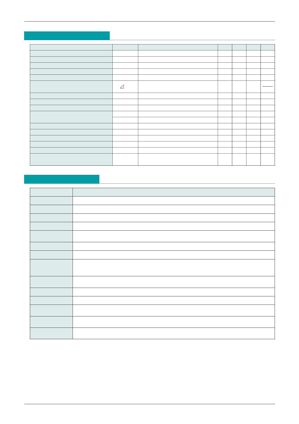
Electrical Characteristics (Except where noted otherwise, Ta=25°C, VCC=5V, SW2, 4, 6, 7 : A) Models listed MM1333
Item
Consumption current 1
Consumption current 2
Consumption current 3
Output voltage 1
Output voltage 2
Output voltage temperature drift
Current limit
CEL-CS leakage current
SW input current
SW input voltage
Low-voltage detection voltage
EXT pin input voltage
EXT pin output voltage
Full-charge detection voltage
Full-charge detection output L
Full-charge detection
output leakage current
Symbol
ICC1
ICC2
ICC3
VO1
VO2
VO
VCL
ICEL
ISW
VL
VH
LV
IS
VEXT
VIC
VCOL
ICO
Measurement conditions
VSW=0V (Charge : ON)
VSW=0V (Charge : ON)
VSW=VCC (Charge : OFF)
Ta=25°C
Ta=0~+40°C
Ta=-20~+70°C
Charge : ON
Charge : OFF
No load
ISINK=0.3mA
Min. Typ. Max. Units
300 400 µA
1.1 1.6 mA
2 4 µA
4.065 4.100 4.135 V
4.050 4.100 4.150 V
±0.25
mV
°C
90 100 110 mV
1 µA
20
µA
-0.3
2.0 V
VCC-1.0
VCC+0.3 V
1.90 2.00 2.10 V
10 20
mA
0.3
VCC-0.3 V
26 31 36 mV
0.2 0.4 V
1 µA
Measurement Method (Except where noted otherwise, Ta=25°C, VCC=5V, SW2 : A, SW4 : A, SW6 : A, SW7 : A)
Item
Measurement Method
Consumption current 1 Set V1=0 V, SW4=B, V4=50mV, V6=4.5V ; switch SW6 from A to B and again to A ; then measure the A8 current ICC1.
Consumption current 2 Set V1=0V, SW4=B, V4=50mV, V6=4.5V ; switch SW6 from A to B and again to A ; then measure the A8 current ICC1.
Consumption current 3 Set V1=VCC, and measure the resulting A8 current ICC3.
Output voltage Set V1=0V, V6=4.5V; switch SW6 from A to B and again to A ; then measure the T6 voltage VO.
Current limit
Set V1=0V, set the voltage V6 about 1V lower than the potential at T6 (output voltage), and set SW6
to B ; then measure the T5 voltage VCL.
CEL-CS leakage current Set VCC=0V, V1=0V; set the voltage V6 to 5V; and set SW6 to B and SW7 to C. Then measure the A6 current ICEL.
SW input current With V1=0V, measure the A1 current ISW1.
Set the voltage V6 1V lower than the T6 potential (output voltage), and set SW6 to B. With the
SW input voltage voltage V1 variable, when the A6 current is 100mA or higher this voltage is equal to the charge-on
voltage (VL), and when the current is within ±10µA it is equal to the charge-off voltage (VH).
Low-voltage Set V1=0 V, set V6 to 1V lower than the T6 potential (output voltage), and set switch SW6 to B. Then
detection voltage gradually lower the voltage V6 ; the voltage V6 at which the A6 current is within ±10µA is LV.
EXT pin input voltage Measure the A7 current IS with V1=0V, SW6 set to B, SW7 set to B, V6=3V, and V7=4V.
EXT pin output voltage Set V1=0 V, SW6 to B, and SW7 to C. The T7 voltage when V6=3V and V6=5V is VEXT.
Full-charge Set V1=0V and SW4 to B. Gradually lower the voltage V4 from 50mV ; the voltage V4 when the T2
detection voltage potential falls to 1V or lower from (VCC-1) V or higher is VIC.
Full-charge
detection output L
Measure the T2 voltage VCOL when V1=0V, SW4 is at B and V4=0V.
Full-charge detection
output leakage current
Measure the A2 current ICO when V1=0V, SW4 is at B, V4=50mV, SW2 is at B, and V2=5V.
Warnings regarding use
1. The following components should be added in preparation for use.
1. A capacitance of several µF or so between VCC and GND
2. A 10µF capacitor between CEL and CS
3. A diode to prevent backflow between the collector of the external PNP transistor and pin 6
4. A current-limiting 150Ω resistor between the base of the external PNP transistor and EXT
2. The full charge detection circuit detects voltages of order several mV, and so no hysteresis is applied.
Chattering will occur, and should be born in mind.
3. There is an internal low-voltage detection circuit. If a voltage of at least 2V is not applied to the CEL pin, no
output will be obtained.
Share Link: 