MP8775 データシートの表示(PDF) - Exar Corporation
部品番号
コンポーネント説明
一致するリスト
MP8775 Datasheet PDF : 8 Pages
| |||
MP8775
ELECTRICAL CHARACTERISTICS TABLE (CONT’D)
Description
Symbol
Min
25°C
Typ
Max
Units
Conditions
AC PARAMETERS
Differential Gain Error
dG
Differential Phase Error
dPH
POWER SUPPLIES
Operating Voltage (AVDD, DVDD)9
VDD
Current (AVDD + DVDD)
IDD
2
%
FS = 4 x NTSC
1
°
FS = 4 x NTSC
5
V
17
25
mA
Does not include ref. current
Notes:
1
aTidenesyatetlrcraomndseeitaiwosnuidrvtehosl(tcVaogRdeEeF(F/t2riag5nu6sr)eitisio3tn.h)s.ebADycNdcLuithreaercrroyinrigs(Ftahigefuuvrneoclt2tiao.)gn.eoTofhftehtheIeNsLaanmearplroolignr giisnrptahuteet (m(VFIaSNx))i..mTuhme
difference between the
distance (in LSBs) from
measured and the
the best fit line to
2 Guaranteed. Not tested.
3 Specified values guarantee functionality. Refer to other parameters for accuracy.
4 --1 dB bandwidth is a measure of performance of the A/D input stage (S/H + amplifier). Refer to other parameters for accuracy within
the specified bandwidth.
5
6
7
8
DtDASRleGe,l epitNFneVpDnsIuNdhatsosninuodhplndauDvttbVheeeDedqDliRiumo.iCdvitaeellsoedanttodtocDc>iorV5cnDunnDiset ca(fFotneirdgdbuDteroGesttN4hr.eeD).s.ouuSlttIwspn.upittuchpt eiDndC. ccauprarecnitotsr
analog
will not
input requires driver with low output
exceed specified limits for any input
resistance.
voltage between
9 AGND and DGND pins are connected through the silicon substrate. Connect together at the package and to the analog ground plane.
Specifications are subject to change without notice
ABSOLUTE MAXIMUM RATINGS (TA = +25°C unless otherwise noted)1, 2, 3
VDD to GND . . . . . . . . . . . . . . . . . . . . . . . . . . . . . . . . . . . . . 7 V
VRT & VRB . . . . . . . . . . . . . . . . . . . . VDD +0.5 to GND --0.5 V
VIN . . . . . . . . . . . . . . . . . . . . . . . . . . VDD +0.5 to GND --0.5 V
All Inputs . . . . . . . . . . . . . . . . . . . . . VDD +0.5 to GND --0.5 V
All Outputs . . . . . . . . . . . . . . . . . . . VDD +0.5 to GND --0.5 V
Storage Temperature . . . . . . . . . . . . . . . . . . . --65 to +150°C
Lead Temperature (Soldering 10 seconds) . . . . . . . +300°C
Package Power Dissipation Rating @ 75°C
SOIC, SSOP, PDIP . . . . . . . . . . . . . . . . . . . . . . . 700 mW
Derates above 75°C . . . . . . . . . . . . . . . . . . . . . . 9 mW/°C
Notes:
1 Stresses above those listed under “Absolute Maximum Ratings” may cause permanent damage to the device. This is a
stress rating only and functional operation at or above this specification is not implied. Exposure to maximum rating
conditions for extended periods may affect device reliability.
2 Any input pin which can see a value outside the absolute maximum ratings should be protected by Schottky diode clamps
(HP5082-2835) from input pin to the supplies. All inputs have protection diodes which will protect the device from short
3
transients outside the supplies of less than 100mA for less than 100ms.
VDD refers to AVDD and DVDD. GND refers to AGND and DGND.
Rev. 3.01
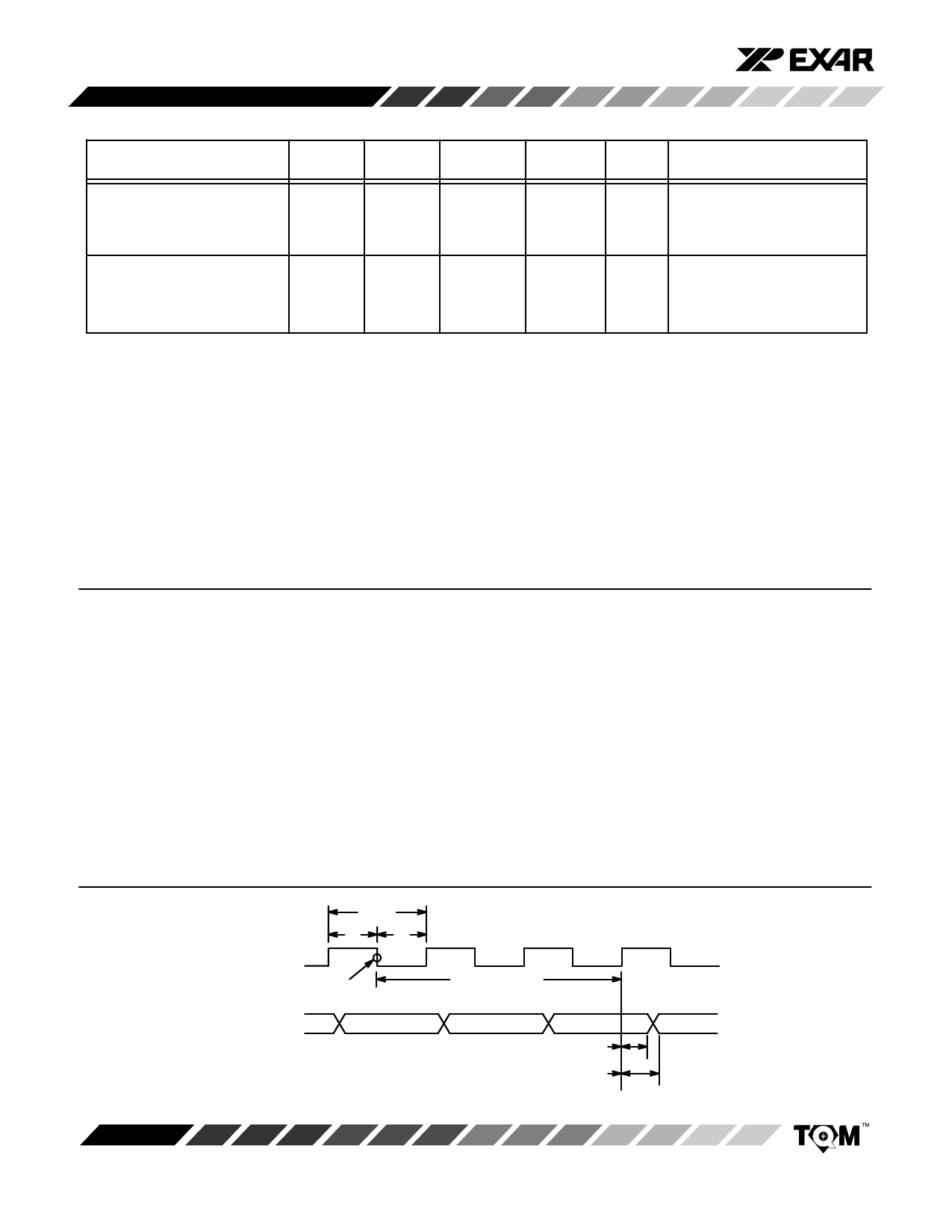
CLK
DATA
1/FS
tPWH
tPWL
Sample “N”
N+1
N+2
PIPELINE DELAY
N -- 3
N -- 2
N -- 1
t HL
t DL
Figure 1. MP8775 Timing Diagram
4
DATA N
Share Link: 