TK11120S データシートの表示(PDF) - Toko America Inc
部品番号
コンポーネント説明
一致するリスト
TK11120S Datasheet PDF : 16 Pages
| |||
TK111xxS
DEFINITION AND EXPLANATION OF TECHNICAL TERMS (CONT.)
Reverse Voltage Protection
ON/OFF RESPONSE WITH CONTROL
Reverse voltage protection prevents damage due to the
output voltage being higher than the input voltage. This
fault condition can occur when the output capacitor remains
charged and the input is reduced to zero, or when an
external voltage higher than the input voltage is applied to
the output side.
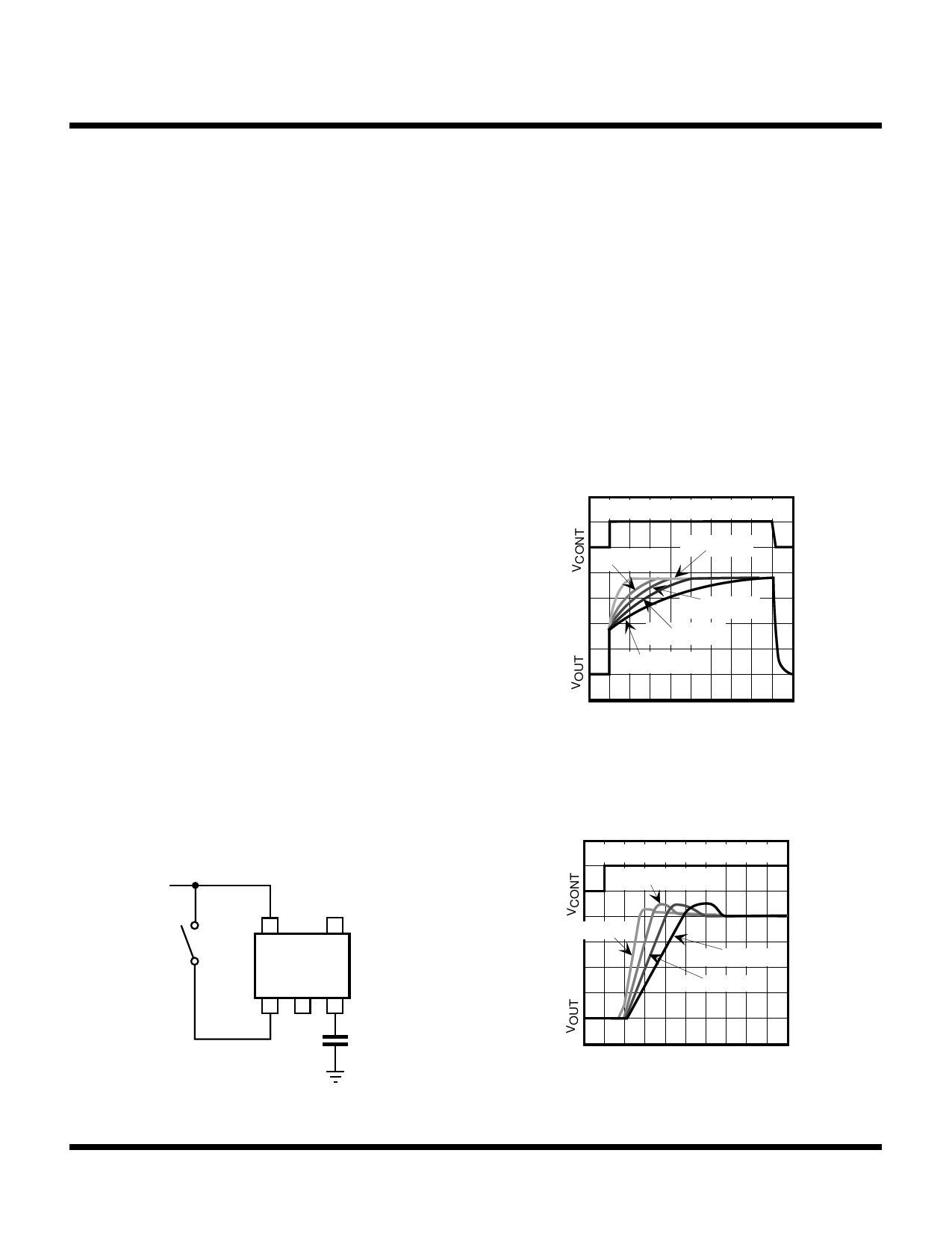
REDUCTION OF OUTPUT NOISE
The turn-on time depends upon the value of the output
capacitor and the noise bypass capacitor. The turn-on time
will increase with the value of either capacitor. The graphs
below show the relationship between turn-on time and
load capacitance. If the value of these capacitors is reduced,
the load and line regulation will suffer and the noise voltage
will increase. If the value of these capacitors is increased,
the turn-on time will increase.
Although the architecture of the Toko regulators is designed
to minimize semiconductor noise, further reduction can be
achieved by the selection of external components. The
obvious solution is to increase the size of the output
capacitor. A more effective solution would be to add a
capacitor to the noise bypass terminal. The value of this
capacitor should be 0.1 µF or higher (higher values provide
greater noise reduction). Although stable operation is
possible without the noise bypass capacitor, this terminal
has a high impedance and care should be taken to avoid
a large circuit area on the printed circuit board when the
capacitor is not used. Please note that several parameters
are affected by the value of the capacitors and bench
testing is recommended when deviating from standard
values.
OUTPUT VOLTAGE RESPONSE B
(OFF→ON)
ILOAD = 30 mA, CL = 2.2 µF
CN = 0.1 µF
CN = 0.33 µF
CN = 0.47 µF
CN = 0.68µF
CN = 1.0 µF
CONTROL FUNCTION
The TK111xxS has an active high control pin. The control
pin requires over 1.8 V for operation and under 0.6 V for
standby. For the range of 0.6 V < VCONT < 1.8 V, operation
is undefined. If the control function is not used, connect the
control pin to VIN.
VIN
0
2
4
6
8
TIME (ms)
OUTPUT VOLTAGE RESPONSE A
(OFF→ON)
ILOAD = 30 mA, CN = 3300 pF
CL = 0.68 µF
CL = 0.47µF
SW
CL = 1.5 µF
CL = 1.0 µF
Page 10
CN
CONTROL FUNCTION
-5
5 15 25 35 45
TIME (µs)
March 1999 TOKO, Inc.
Share Link: 