TGA4541-SM データシートの表示(PDF) - TriQuint Semiconductor
部品番号
コンポーネント説明
一致するリスト
TGA4541-SM Datasheet PDF : 14 Pages
| |||
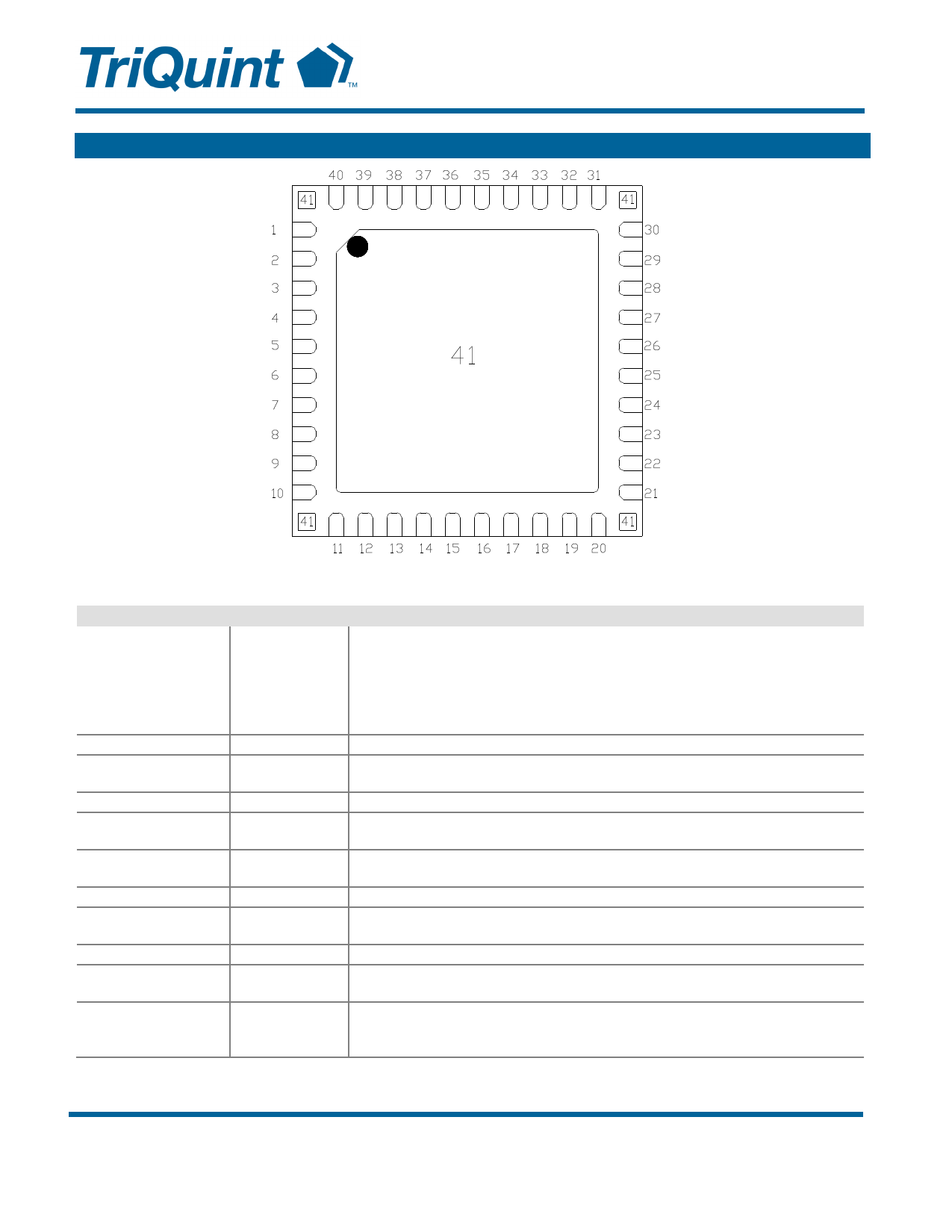
Pin Description
TGA4541-SM
Ka-Band Variable Gain Driver Amplifier
Pin
1, 2, 3, 5, 6, 7, 8, 9,
10, 11, 12, 13, 19,
20, 21, 22, 23, 25,
26, 27, 28, 29, 30,
31, 32, 33, 34, 39,
40
4
14
15, 17, 37
16
Symbol
N/C
RF IN
Vg
N/C
Vd2
18
Vd3
24
RF OUT
35
Vc
36
GND
38
Vd1
41
GND
Top View
Description
No internal connection; must be grounded on PCB.
RF Input.
Gate voltage. Bias network is required; see Application Circuit on page
7 as an example.
No internal connection; should be left open.
Drain voltage. Bias network is required; see Application Circuit on page
7 as an example.
Drain voltage. Bias network is required; see Application Circuit on page
7 as an example.
RF Output.
Control voltage. Bias network is required; see Application Circuit on
page 7 as an example.
Internally grounded through a resistor; must be grounded on PCB.
Drain voltage. Bias network is required; see Application Circuit on page
7 as an example.
Backside paddles; must be grounded on PCB. Multiple vias should be
employed to minimize inductance and thermal resistance; see Mounting
Configuration on page 12 for suggested footprint.
Datasheet: Rev A 08-30-13
© 2013 TriQuint
- 8 of 14 -
Disclaimer: Subject to change without notice
www.triquint.com
Share Link: 