TC74LCX74F データシートの表示(PDF) - Toshiba
部品番号
コンポーネント説明
一致するリスト
TC74LCX74F Datasheet PDF : 10 Pages
| |||
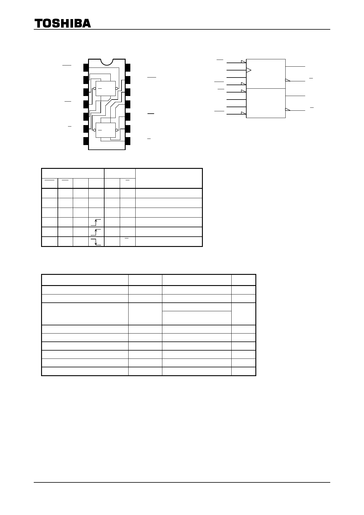
Pin Assignment (top view)
TC74LCX74F/FN/FT/FK
IEC Logic Symbol
1CLR 1
1D 2
1CK 3
1PR 4
1Q 5
1Q 6
GND 7
CK D
QQ
CK D
QQ
14 VCC
13 2CLR
12 2D
11 2CK
10 2PR
9 2Q
8 2Q
1PR 4
1CK 3
1D 2
1CLR 1
2PR 10
2CK 11
2D 12
2CLR 13
S
C1
1D
R
5 1Q
6 1Q
9 2Q
8 2Q
Truth Table
CLR
L
H
L
H
H
H
Inputs
PR D
HX
LX
LX
HL
HH
HX
Outputs
CK Q Q
X
L
H
XHL
XHH
LH
HL
Qn Qn
Function
Clear
Preset
⎯
⎯
⎯
No change
X: Don’t care
Absolute Maximum Ratings (Note 1)
Characteristics
Power supply voltage
DC input voltage
DC output voltage
Input diode current
Output diode current
DC output current
Power dissipation
DC VCC/ground current
Storage temperature
Symbol
VCC
VIN
VOUT
IIK
IOK
IOUT
PD
ICC/IGND
Tstg
Rating
Unit
−0.5 to 7.0
V
−0.5 to 7.0
V
−0.5 to 7.0 (Note 2)
−0.5 to VCC + 0.5
V
(Note 3)
−50
mA
±50 (Note 4) mA
±50
mA
180
mW
±100
mA
−65 to 150
°C
Note 1: Exceeding any of the absolute maximum ratings, even briefly, lead to deterioration in IC performance or
even destruction.
Using continuously under heavy loads (e.g. the application of high temperature/current/voltage and the
significant change in temperature, etc.) may cause this product to decrease in the reliability significantly
even if the operating conditions (i.e. operating temperature/current/voltage, etc.) are within the absolute
maximum ratings and the operating ranges.
Please design the appropriate reliability upon reviewing the Toshiba Semiconductor Reliability Handbook
(“Handling Precautions”/“Derating Concept and Methods”) and individual reliability data (i.e. reliability test
report and estimated failure rate, etc).
Note 2: VCC = 0 V
Note 3: High or low state. IOUT absolute maximum rating must be observed.
Note 4: VOUT < GND, VOUT > VCC
2
2007-10-19
Share Link: 