TC58NVG1S3BFT00 データシートの表示(PDF) - Toshiba
部品番号
コンポーネント説明
一致するリスト
TC58NVG1S3BFT00 Datasheet PDF : 37 Pages
| |||
TC58NVG1S3BFT00/TC58NVG1S8BFT00
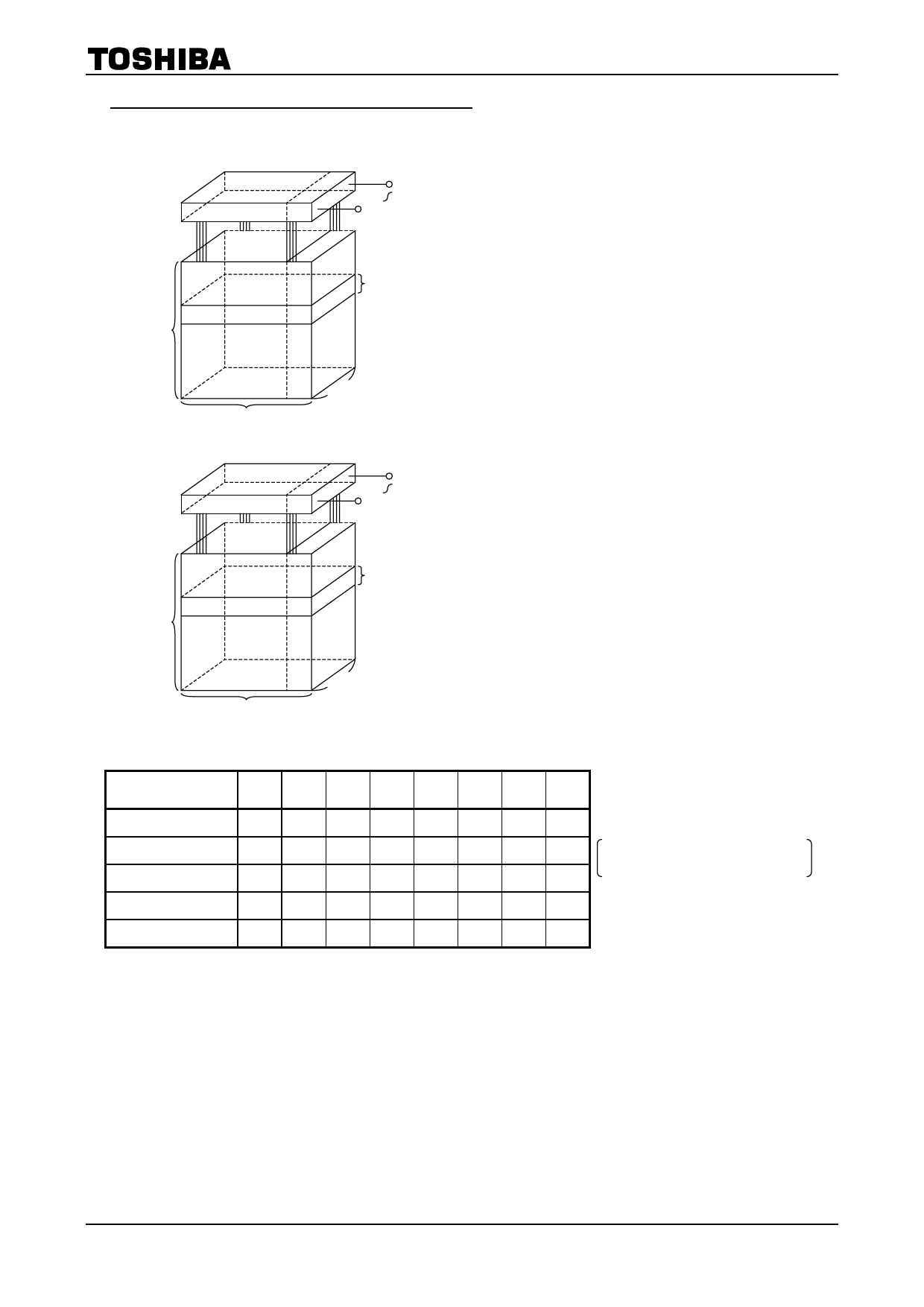
Schematic Cell Layout and Address Assignment
The Program operation works on page units while the Erase operation works on block units.
Page Buffer 2048
131072
pages
2048 blocks
I/O1
64
I/O8
A page consists of 2112 bytes in which 2048 bytes are
used for main memory storage and 64 bytes are for
redundancy or for other uses.
64 Pages = 1 block
1 page = 2112 bytes
1 block = 2112 bytes × 64 pages = (128K + 4K) bytes
Capacity = 2112 bytes × 64pages x 2048blocks
8I/O
2112
Page Buffer 1024
131072
pages
2048 blocks
I/O1
32
I/O16
A page consists of 1056 words in which 1024 words are
used for main memory storage and 32 words are for
redundancy or for other uses.
64 Pages = 1 block
1 page = 1056 words
1 block = 1056 words × 64 pages = (64K + 2K) words
Capacity = 1056 words × 64 pages × 2048 blocks
1056
16I/O
An address is read in via the I/O port over three
consecutive clock cycles, as shown in Table 1.
Table 1. Addressing
First cycle
Second cycle
Third cycle
I/O8 I/O7 I/O6 I/O5 I/O4 I/O3 I/O2 I/O1
CA7 CA6 CA5 CA4 CA3 CA2 CA1 CA0
L
L
L
L CA11 CA10 CA9 CA8
PA7 PA6 PA5 PA4 PA3 PA2 PA1 PA0
CA0 to CA11: Column address
PA0 to PA16: Page address
PA6 to PA16: Block address
PA0 to PA5: NAND address in block
Fourth cycle
PA15 PA14 PA13 PA12 PA11 PA10 PA9 PA8
Fifth cycle
L
L
L
L
L
L
L PA16
Note) I/O9 − 16 must be held low when address is input (×16 device).
17
2003-10-30A
Share Link: 