CXD3027R データシートの表示(PDF) - Sony Semiconductor
部品番号
コンポーネント説明
一致するリスト
CXD3027R Datasheet PDF : 192 Pages
| |||
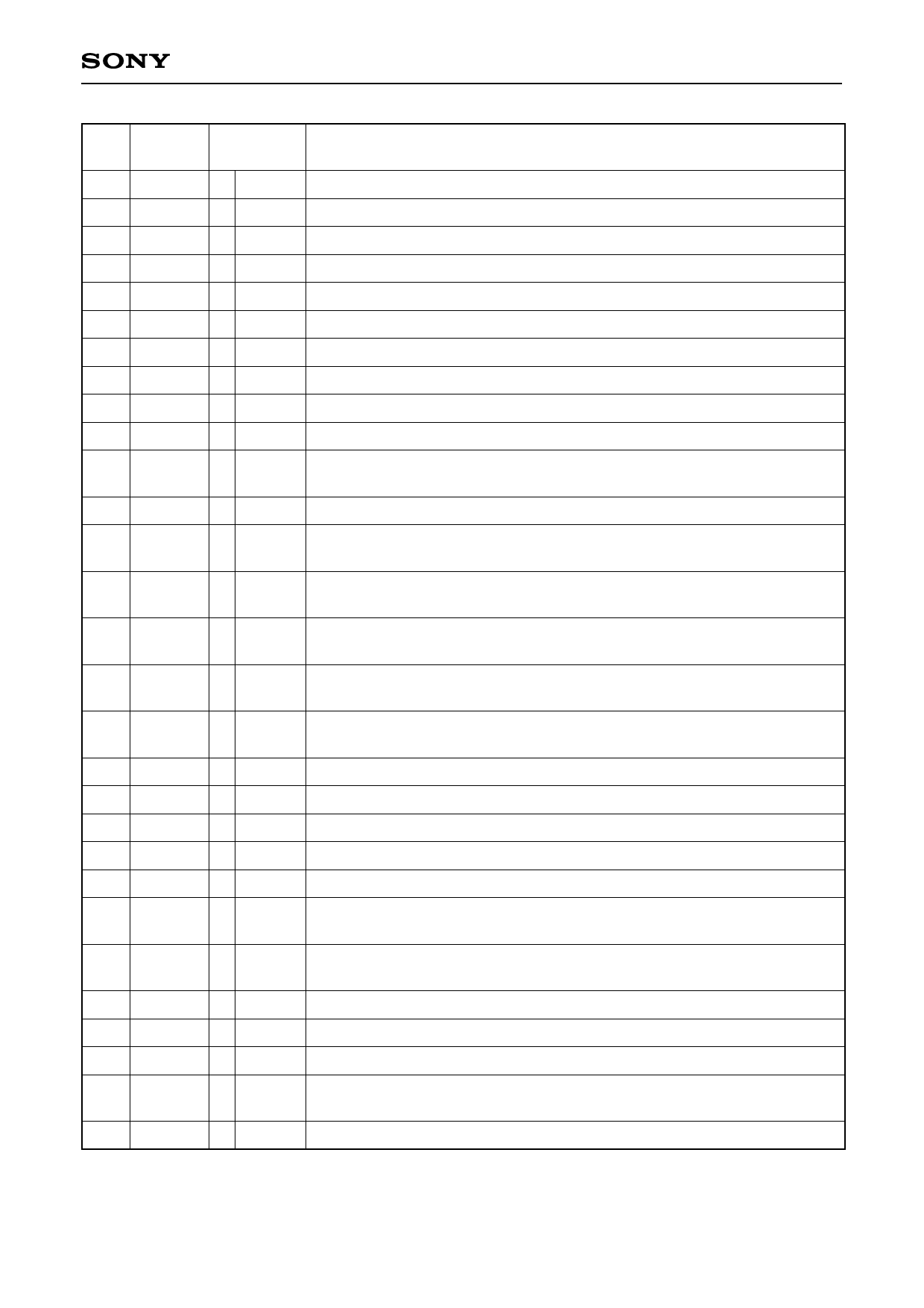
CXD3027R
Pin
No.
Symbol
I/O
Description
66 FILO
O Analog Master PLL filter output (slave = digital PLL).
67 FILI
I
Master PLL filter input.
68 PCO
O 1, Z, 0 Master PLL charge pump output.
69 CLTV
I
Multiplier VCO1 control voltage input.
70 AVSS3 — — Analog GND.
71 RFAC I
EFM signal input.
72 BIAS
I
Asymmetry circuit constant current input.
73 ASYI
I
Asymmetry comparator voltage input.
74 ASYO O 1, 0 EFM full-swing output (low = VSS, high = VDD).
75 AVDD3 — — Analog power supply.
76 XTSL
I
Crystal selection input.
Low when the crystal is 16.9344MHz; high when the crystal is 33.8688MHz.
77 VSS2
— — Digital GND.
78 WDCK
O
1, 0
Word clock output f = 2Fs.
GRSCOR is output by switching with the command.
79 XUGF
O 1, 0
XUGF output.
MNT0, RFCK or SOUT is output by switching with the command.
80 XPCK
O
1, 0
XPCK output.
MNT1 or SOCK is output by switching with the command.
81 GFS
O
1, 0
GFS output.
MNT2, XROF or XOLT is output by switching with the command.
82 C2PO
O
1, 0
C2PO output.
MNT3 or GTOP is output by switching with the command.
83 WFCK O 1, 0 WFCK output.
84 VDD2
— — Digital power supply.
85 DOUT O 1, 0 Digital Out output.
86 LRCK O 1, 0 D/A interface. LR clock output f = Fs.
87 LRCKI I
D/A interface. LR clock input.
88 PCMD
O
1, 0
D/A interface. Serial data output.
(two's complement, MSB first)
89 PDMDI I
D/A interface. Serial data input.
(two's complement, MSB first)
90 BCK
O 1, 0 D/A interface. Bit clock output.
91 BCKI
I
D/A interface. Bit clock input.
92 XVDD
——
Master clock power supply.
93 XTAI
I
Crystal oscillation circuit input.
The master clock is externally input from this pin.
94 XTAO O
Crystal oscillation circuit output.
–6–
Share Link: 