STH18NB40 データシートの表示(PDF) - STMicroelectronics
部品番号
コンポーネント説明
一致するリスト
STH18NB40 Datasheet PDF : 7 Pages
| |||
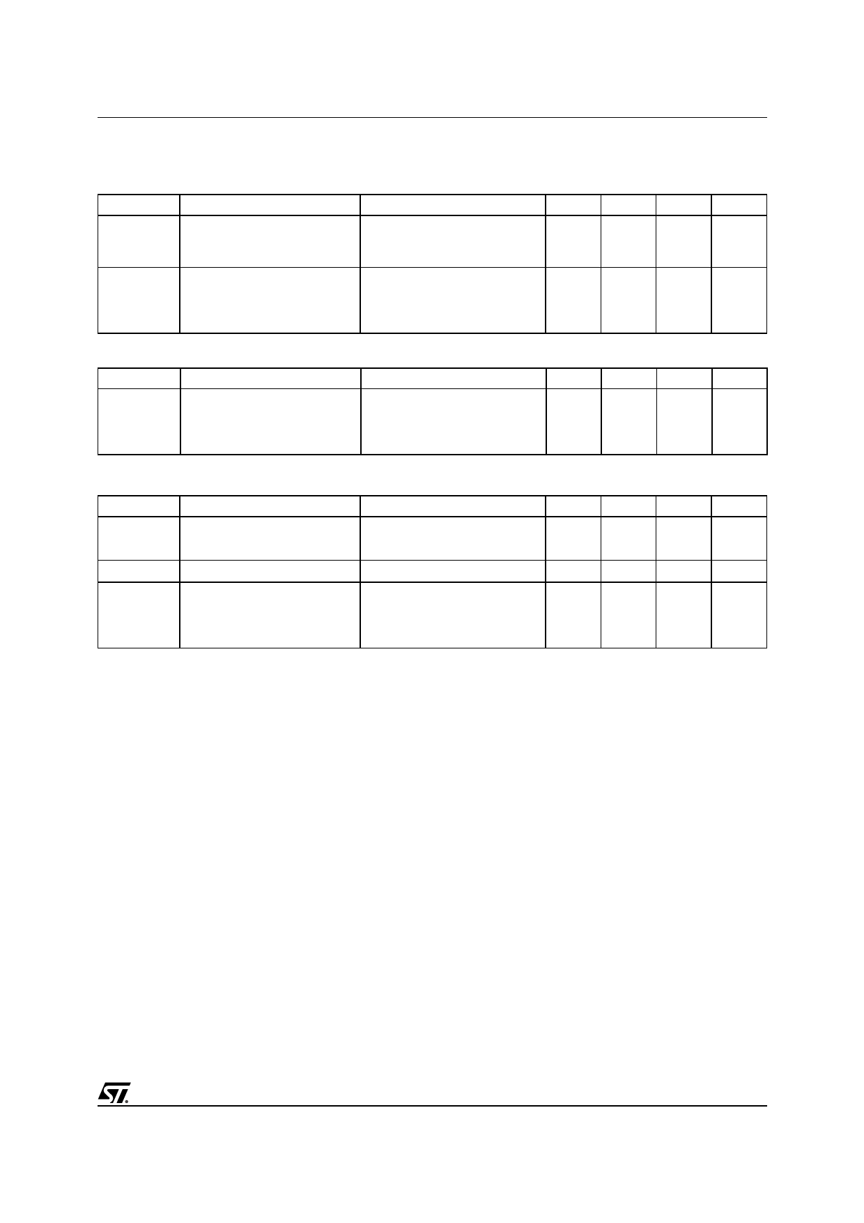
STW18NB40/STH18NB40FI
ELECTRICAL CHARACTERISTICS (CONTINUED)
SWITCHING ON
Symbol
Parameter
td(on)
Turn-on Delay Time
tr
Rise Time
Qg
Total Gate Charge
Qgs
Gate-Source Charge
Qgd
Gate-Drain Charge
Test Conditions
VDD = 200 V, ID = 9.2 A
RG = 4.7Ω VGS = 10 V
(see test circuit, Figure 3)
VDD = 320V, ID = 18.4 A,
VGS = 10V
SWITCHING OFF
Symbol
Parameter
tr(Voff)
Off-voltage Rise Time
tf
Fall Time
tc
Cross-over Time
Test Conditions
VDD = 320V, ID = 18.4 A,
RG = 4.7Ω, VGS = 10V
(see test circuit, Figure 5)
Min. Typ. Max. Unit
27
ns
14
ns
60
84
nC
16
nC
28.3
nC
Min.
Typ.
13
15
27
Max.
Unit
ns
ns
ns
SOURCE DRAIN DIODE
Symbol
Parameter
Test Conditions
ISD
Source-drain Current
ISDM (2) Source-drain Current (pulsed)
VSD (1) Forward On Voltage
ISD = 18.4 A, VGS = 0
trr
Qrr
IRRM
Reverse Recovery Time
Reverse Recovery Charge
Reverse Recovery Current
ISD = 18.4 A, di/dt = 100A/µs,
VDD = 100V, Tj = 150°C
(see test circuit, Figure 5)
Note: 1. Pulsed: Pulse duration = 300 µs, duty cycle 1.5 %.
2. Pulse width limited by safe operating area.
Min.
Typ.
480
5.5
23
Max.
18.4
73.6
1.6
Unit
A
A
V
ns
µC
A
3/7
Share Link: 