STV1601A データシートの表示(PDF) - STMicroelectronics
部品番号
コンポーネント説明
一致するリスト
STV1601A Datasheet PDF : 17 Pages
| |||
STV1601A
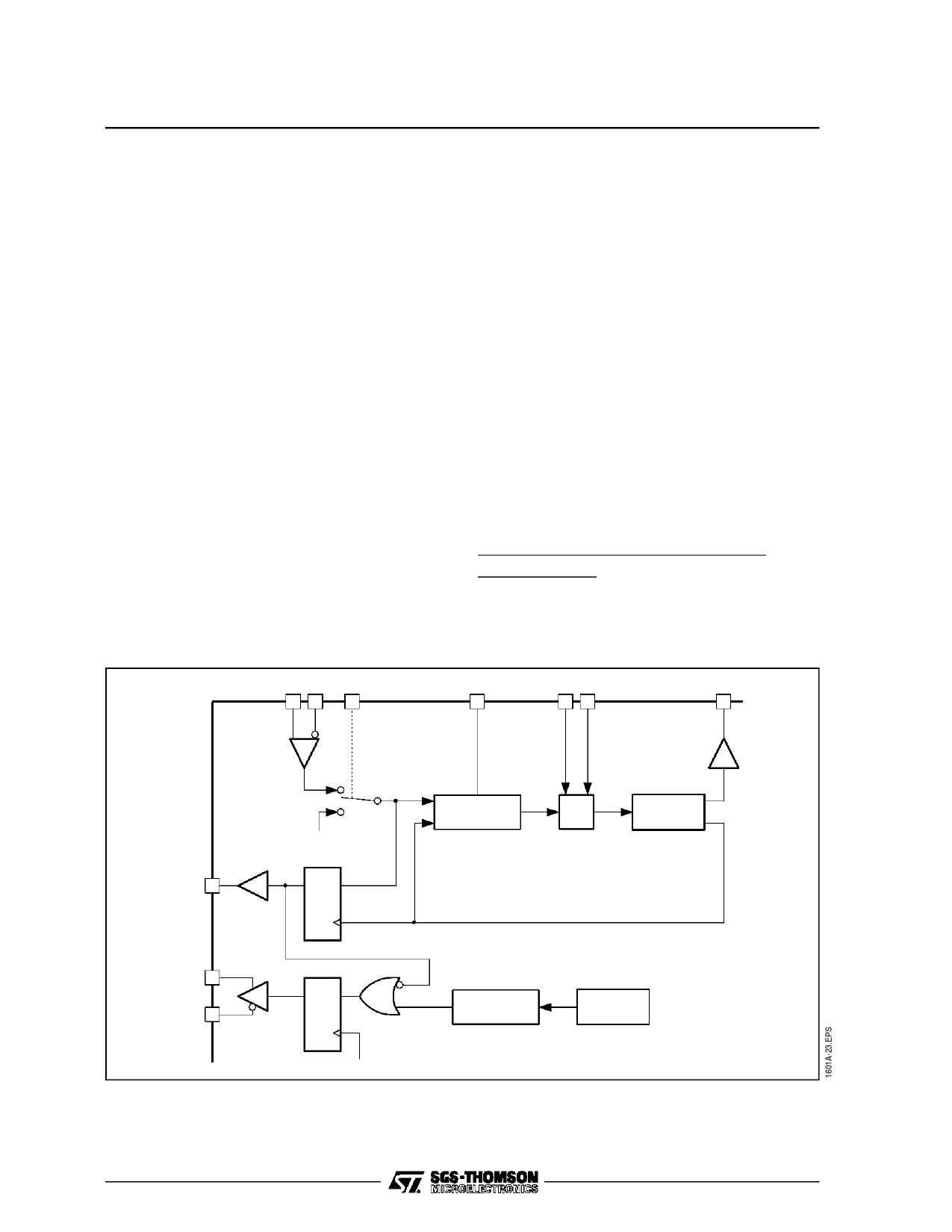
3. PLL block
PARALLEL CLOCK INPUT CONTROL
PLL, PLL lock detection and the various blocks of
the serial output control are shown in Figure 13.
When TN1 is connected to GND (set High), the
parallel clock input is disabled.
The VCO turns to free running conditions and its
frequency can be adjusted through FV.
This frequency decreases when the resistor value
between FV and VEE is reduced. Oscillation fre-
quency monotoring is performed through PCK
which delivers a frequency divided by ten.
When PLL is locked, PLL and PCX input signal
phases are nearly matched. The RC network con-
nected to TN1, temporarily, disables the parallel
clock in order to avoid mislocking problems.
VCO oscillation frequency range selection is avail-
able through RSE ; High : from 140 to 270MHz ;
Low : from 100 to 145MHz.
TRP (Pin 34) is the phase comparator output. To
minimize jitter, a trap circuit, consisting in a serial
tuned circuit at parallel clock frequency can be
used.
Figure 13 : PLL and Serial Output Control Block
PLL LOCK DETECTION
The LST signal is generated by latching the incom-
ing parallel clock by the internal one (which is 1/10
of the VCO frequency). LST is used as a PLL lock
detection signal and also controls the serial output.
If the parallel clock input is disabled (by means of
TN1), LST turns Low and the serial output is dis-
abled as described in the previous section (SX
(Pin 3) = High, SY (Pin 4) = Low).
If the serial output has to be disabled while no
parallel clock input is provided, PCX must be set
Low and PCY must be set High.
4. Sync word
To convert serial data back to parallel, insertion of
some timing reference data indicating the parallel
data word boundary in the serial data is needed.
This, called TRS (Timing Reference Signal) in the
digital interface format, consists of the three con-
secutive words 3FFH, 000H, 000H.
Conversion to 10-bit TRS from 8-bit (TRS)
8-bit parallel data
8-bit parallel data can be converted into 10-bit data
by using the 8th bit as the MSB and by setting the
2 LSBs at logical states as shown in Figure 14.
PCY PCX TN1
TRP
FV RSE
PCK
LST
SX
SY
12/17
”0”
QD
P HA S E
COMP ARATOR
VCO
1/10 DIVIDER
QD
Serial Clock
NRZ To NRZI
CONVERSION
SCRAMBLER
Share Link: 