SMD5962-92324 データシートの表示(PDF) - Cypress Semiconductor
部品番号
コンポーネント説明
一致するリスト
SMD5962-92324 Datasheet PDF : 15 Pages
| |||
STK11C68-5 (SMD5962-92324)
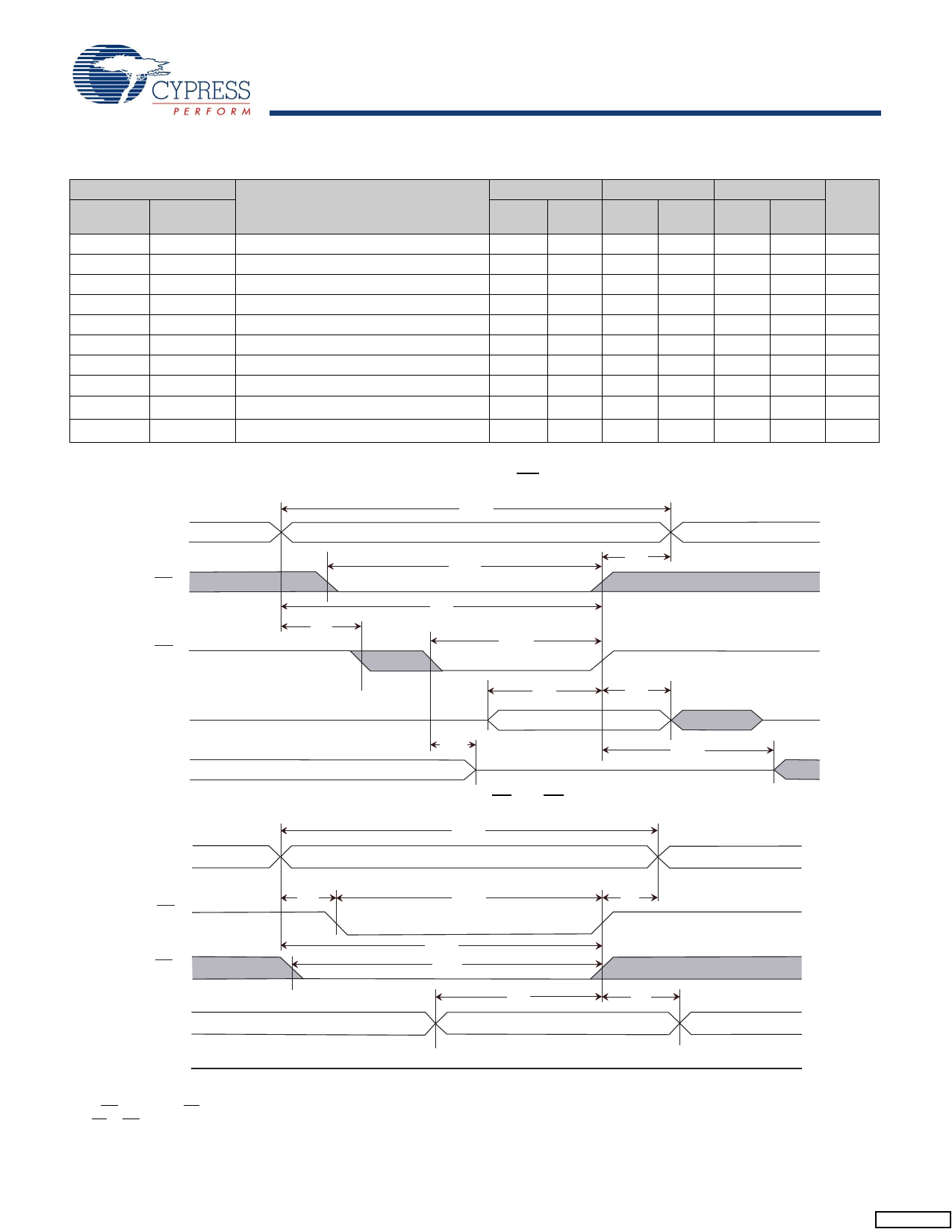
SRAM Write Cycle
Parameter
Cypress
Parameter
Alt
Description
tWC
tPWE
tSCE
tSD
tHD
tAW
tSA
tHA
tHZWE [6,7]
tLZWE [6]
tAVAV
Write Cycle Time
tWLWH, tWLEH Write Pulse Width
tELWH, tELEH Chip Enable To End of Write
tDVWH, tDVEH Data Setup to End of Write
tWHDX, tEHDX Data Hold After End of Write
tAVWH, tAVEH Address Setup to End of Write
tAVWL, tAVEL Address Setup to Start of Write
tWHAX, tEHAX Address Hold After End of Write
tWLQZ
Write Enable to Output Disable
tWHQX
Output Active After End of Write
35 ns
Min Max
35
25
25
12
0
25
0
0
13
5
45 ns
Min Max
45
30
30
15
0
30
0
0
15
5
Switching Waveforms
Figure 8. SRAM Write Cycle 1: WE Controlled [7, 8]
tWC
ADDRESS
tSCE
tHA
CE
tAW
tSA
WE
tPWE
55 ns
Min Max
55
45
45
30
0
45
0
0
35
5
Unit
ns
ns
ns
ns
ns
ns
ns
ns
ns
ns
DATA IN
DATA OUT
ADDRESS
PREVIOUS DATA
tHZWE
tSD
DATA VALID
HIGH IMPEDANCE
tHD
tLZWE
Figure 9. SRAM Write Cycle 2: CE and OE Controlled [7, 8]
tWC
tSA
tSCE
tHA
CE
WE
DATA IN
tAW
tPWE
tSD
tHD
DATA VALID
DATA OUT
HIGH IMPEDANCE
Notes
7. If WE is Low when CE goes Low, the outputs remain in the high impedance state.
8. CE or WE must be greater than VIH during address transitions.
Document Number: 001-51001 Rev. *A
Page 8 of 15
[+] Feedback
Share Link: 