ST7554 データシートの表示(PDF) - STMicroelectronics
部品番号
コンポーネント説明
一致するリスト
ST7554 Datasheet PDF : 11 Pages
| |||
ST7554
PIN DESCRIPTION
1 - Power Supply (7 pins)
1.1 - Regulator Input Power Supply (VBUS)
This pin must be connected to USB VBUS (+5V).
It supplies the integrated analog USB transceiver.
It is also the positive regulator power supply input
(5V) when ST7554 is in bus-powered mode
(PSM = 1) and it is used to internally generate the
3.3V supply for the digital and analog circuitry.
1.2 - Regulated Analog VDD Supply (VREGA)
This pin is the analog power supply input (PSM = 0)
or analog 3.3V power supply output (PSM = 1).
This pin is the positive analog power supply for the
external Codec and DAA.
It is recommended to add a 1µF capacitor between
VREGA and GNDA as close as possible to the
IC pins.
1.3 - Regulated VDD Supply (VREGD)
This pin is the digital power supply input (PSM = 0)
or digital 3.3V power supply output (PSM = 1).
This pin is the positive digital power supply for the
external Codec and DAA.
It is recommended to add a 1µF capacitor between
VREGA and GNDA as close as possible to the
IC pins.
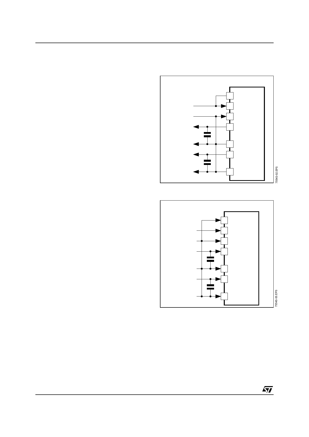
1.4 - Power Supply Mode (PSM)
This pin controls the VREGD and VREGA power
supply mode.
When PSM = 1, the application is bus-powered.
The 3.3V power supply is generated internally from
VBUS. In this case VREGD and VREGA are out-
puts which can be used to supply 3.3V to external
devices (see Figure 1).
When PSM = 0, the application is self-powered.
VBUS must be still connected to the VBUS Pin of
the USB connector in order to supply the integrated
USB transceiver. Anyway in this case VREGD and
VREGA must be fed by a 3.3V externally regulated
digital and analog power supplies (see Figure 2).
1.5 - Ground (DGND, AGND and GNDBUS)
DGND, AGND and GNDBUS are the digital, analog
and USB ground return pins respectively.
They should be connected together outside the
chip to the GND pin of the USB plug.
Figure 1 : ST7554 in Bus-Powered mode
(PSM = 1)
ST7554
from USB
to other
digital ICs
to other
analog ICs
8 PSM
5 VBUS
3 GNDBUS
4 VREGD
32 DGND
6 VREGA
7 AGND
Figure 2 : ST7554 in Self Powered mode
(PSM = 0)
ST7554
from USB
8 PSM
5 VBUS
3 GNDBUS
4 VREGD
from 3.3V
externally
regulated
supplies
32 DGND
6 VREGA
7 AGND
2 - USB Interface (D+ , D-)
These pins are the positive and negative USB
differential data lines. They shall be both connected
to the USB plug or USB protection circuit via 27Ω
series resistors for line impedance matching.
4/11
Share Link: 