TSM108 データシートの表示(PDF) - STMicroelectronics
部品番号
コンポーネント説明
一致するリスト
TSM108 Datasheet PDF : 13 Pages
| |||
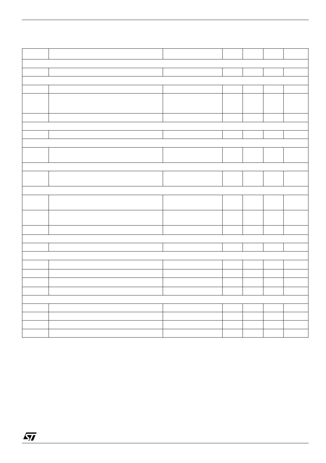
TSM108
ELECTRICAL CHARACTERISTICS
Tamb = 25°C, VCC + 12V (unless otherwise specified)
Symbol
Parameter
Test Condition
Min. Typ. Max. Unit
CURRENT CONSUMPTION
ICC Current Consumption
STANDBY
4
7
mA
Istby Current Consumption in Standby Mode
150
µA
Vsh Input Standby Voltage High Impedance
Internal Pull up resistor. 2
V
Stby pin should be left
open
Vsl Input Standby Voltage Low
OSCILLATOR
0.8
V
FOSC Frequency of the Oscilator
VOLTAGE CONTROL 1) 2)
COSC = 220pF
70 100 130 kHz
Vref Voltage Control Reference
CURRENT CONTROL 3) 4) 5)
Tamb = 25°C
2.520
V
-25°C < Tamb < 85°C 2.450
2.590
Vsense Current Control Reference Voltage
Tamb = 25°C
196 206 216 mV
-25°C < Tamb < 85°C
191
221
GATE DRIVE - P CHANNEL MOSFET DRIVE
Isink Sink Current - Switch ON
Isource Source Current - Swith OFF
Cload Input Capacitance of the PMOSFET 6)
Tamb = 25°C
-25°C < Tamb < 85°C
Tamb = 25°C
-25°C < Tamb < 85°C
40
mA
15
80
mA
30
1
1.5
nF
PWM
∆max.
UVLO
Maximum Duty Cycle of the PWM function
95 100
%
UV Under Voltage Lock Out 7)
-25°C < Tamb < 85°C
8
9
V
UVhyst UVLO Voltage Hysteresis - low to high
Ruvl Upper Resistor of UVLO bridge 8)
Tamb = 25°C
200
mV
184
kΩ
Ruvl
OVLO
Lower Resistor of UVLO bridge (see note 8)
Tamb = 25°C
76.5
kΩ
OV Over Voltage Lock Out (see note 7)
-25°C < Tamb < 85°C
32
35
V
OVhyst OVLO Voltage Hysteresis - low to high
400
mV
Rovl Upper Resistor of OVLO bridge (see note 8) Tamb = 25°C
275
kΩ
Rovl Lower Resistor of OVLO bridge (see note 8) Tamb = 25°C
23.2
kΩ
1. Vref parameter indicates global precision of the voltage control loop.
2. Control Gain : Av = 95dB ; Input Resistance : Rin = infinite ; Output Resistance : Rout = 700MΩ ; Output Source/Sink Current :
Iso, Isi = 150µA ; Recommended values for the compensation network are : 22nF & 22kΩ in series between output and ground.
3. Vsense parameter indicated global precision of the current control loop.
4. Control Gain : Av = 105dB ; Input Resistance : Rin =380kΩ ; Output Resistance : Rout = 105MΩ ; Output Source/Sink Current :
Iso, Isi = 150µA ; Recommended values for the compensation network are : 22nF & 22kΩ in series between output and ground.
5. A current foldback function is implemented thanks to a systematic -6mV negative offset on the current amplifier inputs which
protects the battery from over charging current under low battery voltage conditiions, or output short circuit conditions.
6. The Gate Drive output stage has been optimized for PMosfets with input capacitance equal to Cload. A bigger Mosfet (with input
capacitance higher than Cload) can be used with TSM108, but the gate drive performances will be reduced (in particular when
reaching the Dmax. PWM mode).
7. The given limits comprise the hysteresis (UVhyst).
8. It is possible to modify the UVLO and OVLO limits by adding a resistor (to ground or to VCC) on the pins UV and OV.
The internal values of the resistor should be taken into account.
3/13
Share Link: 