SC4605 データシートの表示(PDF) - Semtech Corporation
部品番号
コンポーネント説明
一致するリスト
SC4605 Datasheet PDF : 19 Pages
| |||
SC4605
POWER MANAGEMENT
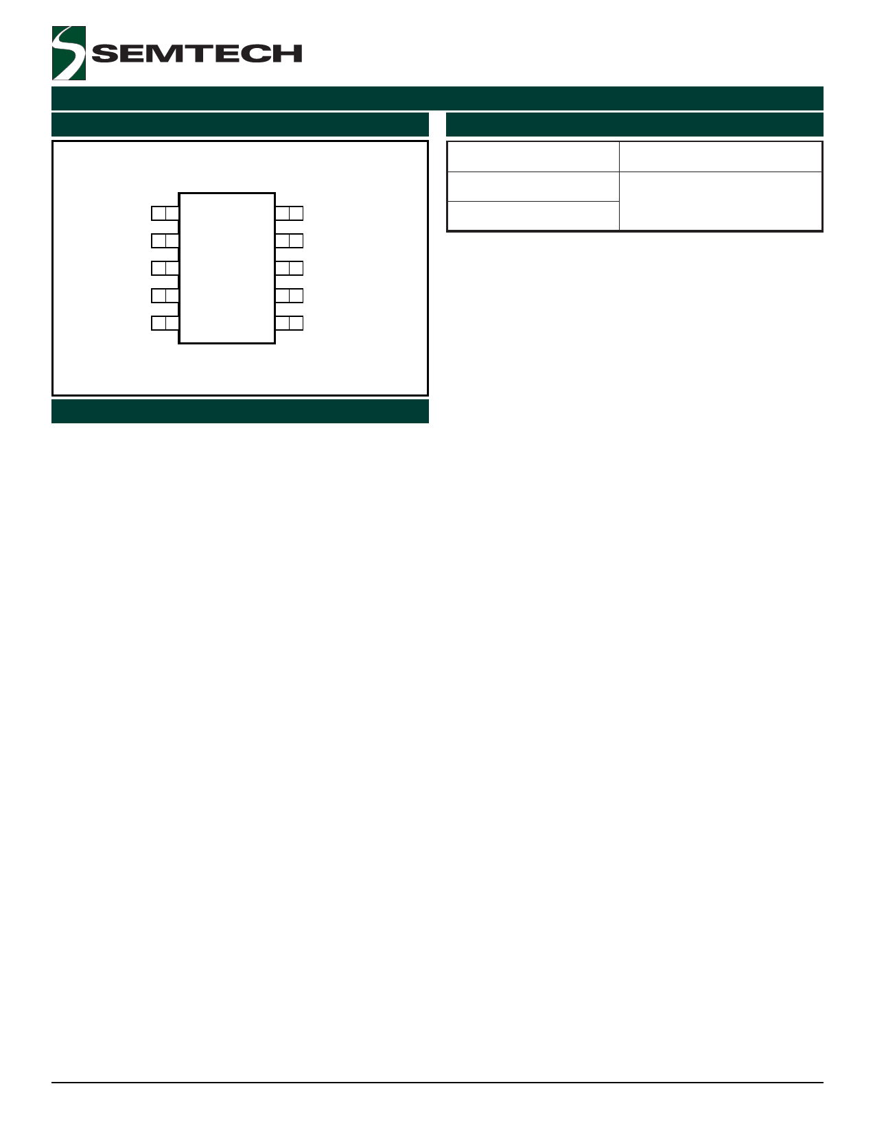
Pin Configuration
TOP VIEW
BST
1
VCC
2
ISET
3
COMP
4
FS/SYNC
5
10
DRVH
9
PHASE
8
DRVL
7
GND
6
VSENSE
Ordering Information
Part Number (1)
SC4605IMSTR
SC4605IMSTRT (2)
Device
MSOP-10
Notes:
(1) Only available in tape and reel packaging. A reel
contains 2500 devices.
(2) Lead free product. This product is fully WEEE and
RoHS compliant.
(MSOP-10)
Pin Descriptions
VCC: Positive supply rail for the IC. Bypass this pin to
GND with a 0.1 to 4.7µF low ESL/ESR ceramic capaci-
tor.
GND: All voltages are measured with respect to this pin.
All bypass and timing capacitors connected to GND should
have leads as short and direct as possible.
FS/SYNC: A capacitor from FS pin to GND sets the PWM
oscillator frequency. Use a high quality ceramic capacitor
with low ESL and ESR for best result. A minimum capaci-
tor value of 200pF ensures good accuracy and less sus-
ceptibility to circuit layout parasitics. When the FS is pulled
and held below 0.2V, its sleep mode operation is invoked.
The Sleepmode supply current is 10µA typical. The oscil-
lator and PWM are designed to provide practical opera-
tion up to 600kHz. In synchronous mode operation, a
low value resistor has to be connected between ground
and the timing capacitor. An external clock is then feed
into the resistor capacitor junction to override the inter-
nal clock.
VSENSE: This pin is the inverting input of the voltage
amplifier and serves as the output voltage feedback point
for the Buck converter. It senses the output voltage through
an external divider.
ISET / PHASE: PHASE is connected to the junction be-
tween the two external power MOSFET transistors. The
voltage drop across the high side MOSFET during its con-
duction is compared with the voltage drop generated by
the internal 50µA current source and the external cur-
rent limit resistor connected between PHASE and Vin,
and forms the current limit comparator and logic sets
the PWM latch and terminates the output pulse. If the
converter output voltage drops below 68.75% of its nomi-
nal voltage, the controller stops switching and goes
through a soft start sequence. This prevents excess
power dissipation in the low side MOSFET during a short
circuit. The current limit threshold is set by the external
resistor between VCC and ISET.
BST: This pin connects the external charge pump, and
powers the high side MOSFET gate drive.
DRVH, DRVL: The output drivers are rated for 1A peak
currents. The PWM circuitry provides complementary drive
signals to the output stages. The cross conduction of
the external MOSFETs is prevented by monitoring the
voltage on the driver pins of the MOSFET pair in conjunc-
tion with a time delay optimized for FET turn-off charac-
teristics.
COMP: This is the output of the voltage amplifier. The
voltage at this output is inverted internally and connected
to the non-inverting input of the PWM comparator. A lead-
lag network around the voltage amplifier compensates for
the two pole LC filter characteristic inherent to voltage mode
control and is required in order to optimize the dynamic
performance of the voltage mode control loop.
2004 Semtech Corp.
4
www.semtech.com
Share Link: 