SC4603(2004) データシートの表示(PDF) - Semtech Corporation
部品番号
コンポーネント説明
一致するリスト
SC4603 Datasheet PDF : 16 Pages
| |||
SC4603
POWER MANAGEMENT
Applications Information - (Cont.)
For a low voltage and high output current application such
as the 3.3V/1.5V@6A case, the conduction loss is often
dominant and selecting low R MOSFETs will notice-
DS(ON)
ably improve the efficiency of the converter even though
they give higher switching losses.
The gate charge loss portion of the top/bottom MOSFET’s
total power loss is derived from the SC4603. This gate
charge loss is based on certain operating conditions
(fs, VGATE, and IO).
The thermal estimations have to be done for both
MOSFETs to make sure that their junction temperatures
do not exceed their thermal ratings according to their
total power losses P , ambient temperature T and their
TOTAL
A
thermal resistances RθJA as follows:
TJ(max)
<
TA
+
PTOTAL
R θJA
Loop Compensation Design:
For example, if
VREF @ 2.25V =
VCC = 2.25V, the reference voltage,
V @ 3.3V
REF
+
Vref @ 3.3V
100
•
Change @2.25V • VCC − 3.3V =
Internal Reference
500
+
500
100
•
0.1•
2.25
−
3.3
=
500.5(mV )
C2
C1
5 FS
1 VCC
2 SYNC
3 COMP
4 VSENSE
ISET 6
PDRV 10
PHASE 7
NDRV 9
GND 8
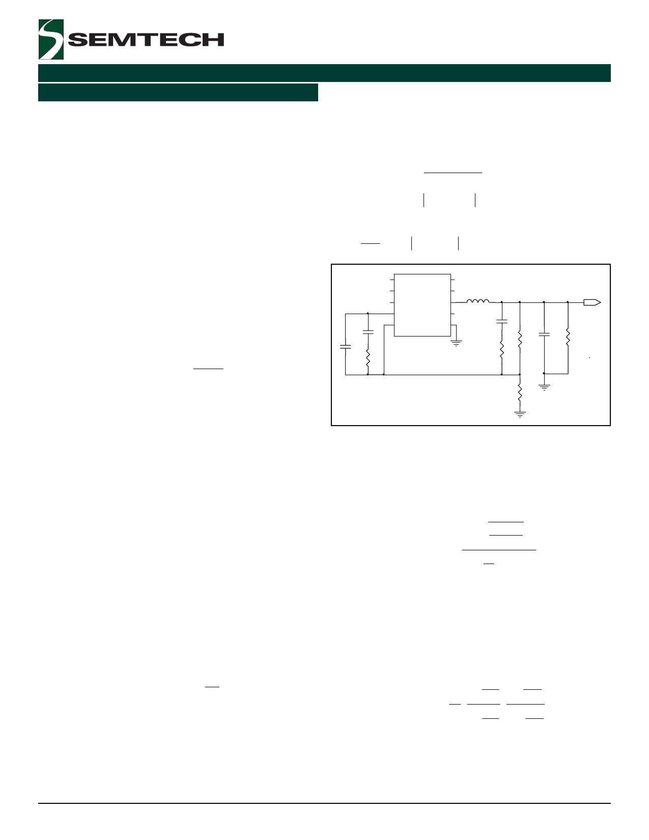
SC4603
R1
L1
C9
R8
Vout
C4
R
R7
R9
For a DC/DC converter, it is usually required that the
converter has a loop gain of a high cross-over frequency
for fast load response, high DC and low frequency gain
for low steady state error, and enough phase margin for
its operating stability. Often one can not have all these
properties at the same time. The purpose of the loop
compensation is to arrange the poles and zeros of the
compensation network to meet the requirements for a
specific application.
The SC4603 has an internal error amplifier and requires
the compensation network to connect among the COMP
pin and VSENSE pin, GND, and the output as shown in
Figure 3. The compensation network includes C1, C2,
R1, R7, R8 and C9. R9 is used to program the output
voltage according to:
VOUT
=
0.5
⋅
(1
+
R
R
7
9
)
As indicated in Internal Reference Change section, the
internal reference voltage (measured at VSENSE pin)
changes slightly if the input voltage of the SC4603 is
away from 3.3V.
Figure 3. Compensation network provides 3 poles and
2 zeros.
For voltage mode step down applications as shown in
Figure 3, the power stage transfer function is:
1+
s
1
G VD (s)
=
VIN
1+
s
RC
L1
R
+
⋅ C4
s2L1C4
Where:
R = load resistance and
RC = C4’s ESR.
The compensation network will have the characteristic
as follows:
1+ s 1+ s
GCOMP (s) =
ωI
s
⋅
1+
ωZ1
s
⋅
⋅1+
ωZ2
s
ωP1
ωP2
2004 Semtech Corp.
11
www.semtech.com
Share Link: 