SC16315S データシートの表示(PDF) - Silan Microelectronics
部品番号
コンポーネント説明
一致するリスト
SC16315S Datasheet PDF : 12 Pages
| |||
SC16315S
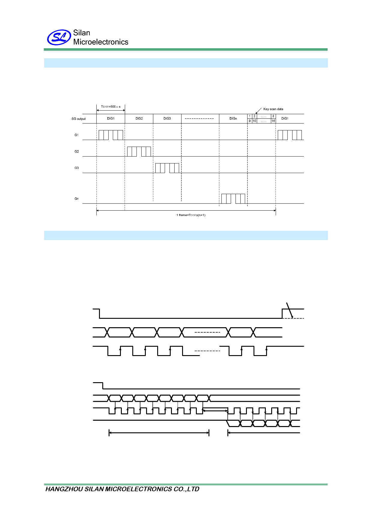
KEY SCANNING AND DISPLAY TIMING
The Key Scanning and display timing diagram is given below. One cycle of key scanning consists of 2 frames.
The data of the 8 x 2 matrix is stored in the RAM.
Figure 11: SC16315S scanning & display timing diagram
SERIAL COMMUNICATION FORMAT
The following diagram shows the SC16315S serial communication format. The DOUT Pin is an N- channel,
open-drain output pin; therefore, it is highly recommended that an external pull-up resistor (1 KΩ to 10 KΩ) must
be connected to DOUT.
Figure 12: SC16315S serial communication format
Reception (command/data write)
If data continues
STB
DIN
b0
b1
b2
b6
b7
CLK
1
2
3
7
8
Transmission (data read)
STB
DIN
b0 b1 b2 b3 b4 b5 b6 b7
CLK
DOUT
12345678
tWAIT
123456
b0 b1 b2 b3 b4 b5
Data read command is set.
Data reading starts
Where: twait (waiting time) ≥ 1µs.
It must be noted that when the data is read, the waiting time (twait) between the rising of the eighth clock that
has set the command and the falling of the first clock that has read the data is greater or equal to 1µs.
HANGZHOU SILAN MICROELECTRONICS CO.,LTD
Http: www.silan.com.cn
REV:1.2 2004.03.01
Page 7 of 13
Share Link: 