RPM872-H12 データシートの表示(PDF) - ROHM Semiconductor
部品番号
コンポーネント説明
一致するリスト
RPM872-H12 Datasheet PDF : 7 Pages
| |||
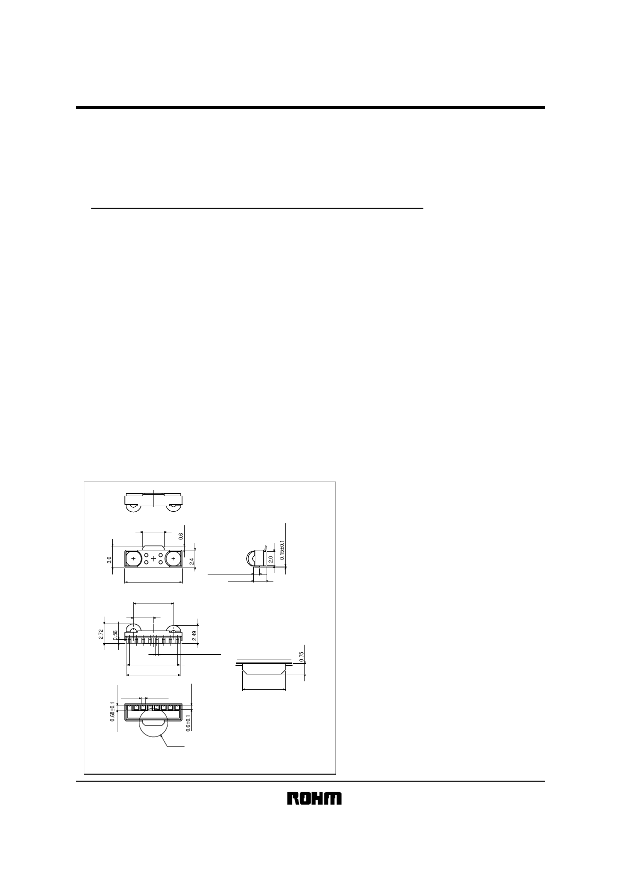
Photo Link Module
RPM872-H12
zNotes
1) VLEDA (8pin), VCC (3pin) and VIO (2pin)
• Other power source can be used difference between VLEDA and VCC and VIO.
(VIO < VCC + 0.3V)
2) Caution in designing board lay-out
To get maximum potential from RPM872-H12, please keep in mind following instruction.
• The line of RXD (6pin) should be connected at backside via through hole close to RPM872-H12 pin lead. Better not to
be close to photo diode side (1pin).
⇒This is to minimize feedback supplied to photo diode from RXD.
• As for C1 between 3-4 pin should be placed close to RPM872-H12.
• Better to be placed more than 1.0cm in radius from photo diode (pin1 side) and also away from the parts which
generates noise, such as DC / DC converter.
3) Others
• Please be sure to set up the TXD (7pin) input to be “L” (under 0.3V) except transmitting data
(for < 90µs, on duty < 20%).
• Power down current might increase if exposed by strong light (ex. direct sunlight) at powerdown mode.
• Please use by the signal format which is specified by IrDA Ver1.2 (Low Power).
• There might be on error if used by different signal format.
• Please pay attention to the lens carefully. Dusts of scratch on the lens may effect the characteristics of product.
Please handle it with care.
4) Eye safe
• IEC825-1 (EN60825-1) Class 1 Eye Safe.
zExternal dimensions (Unit : mm)
3.0
PinPD
LED
8.0
0.84±0.1
1.75
5.6
2.8
1
P0.95×7=6.65
7.6
0.6±0.1
8
0.37±0.1
A Part Size (Shield Case underside size)
3.0
NOTE
TOLERANCE±0.2mm
COPLANARITY:0.1mmMAX
A
UNIT:mm
ETH450
Rev.A
6/6
Share Link: 