RJH60D3DPE(2009) データシートの表示(PDF) - Renesas Electronics
部品番号
コンポーネント説明
一致するリスト
RJH60D3DPE Datasheet PDF : 4 Pages
| |||
RJH60D3DPE
Preliminary
Electrical Characteristics
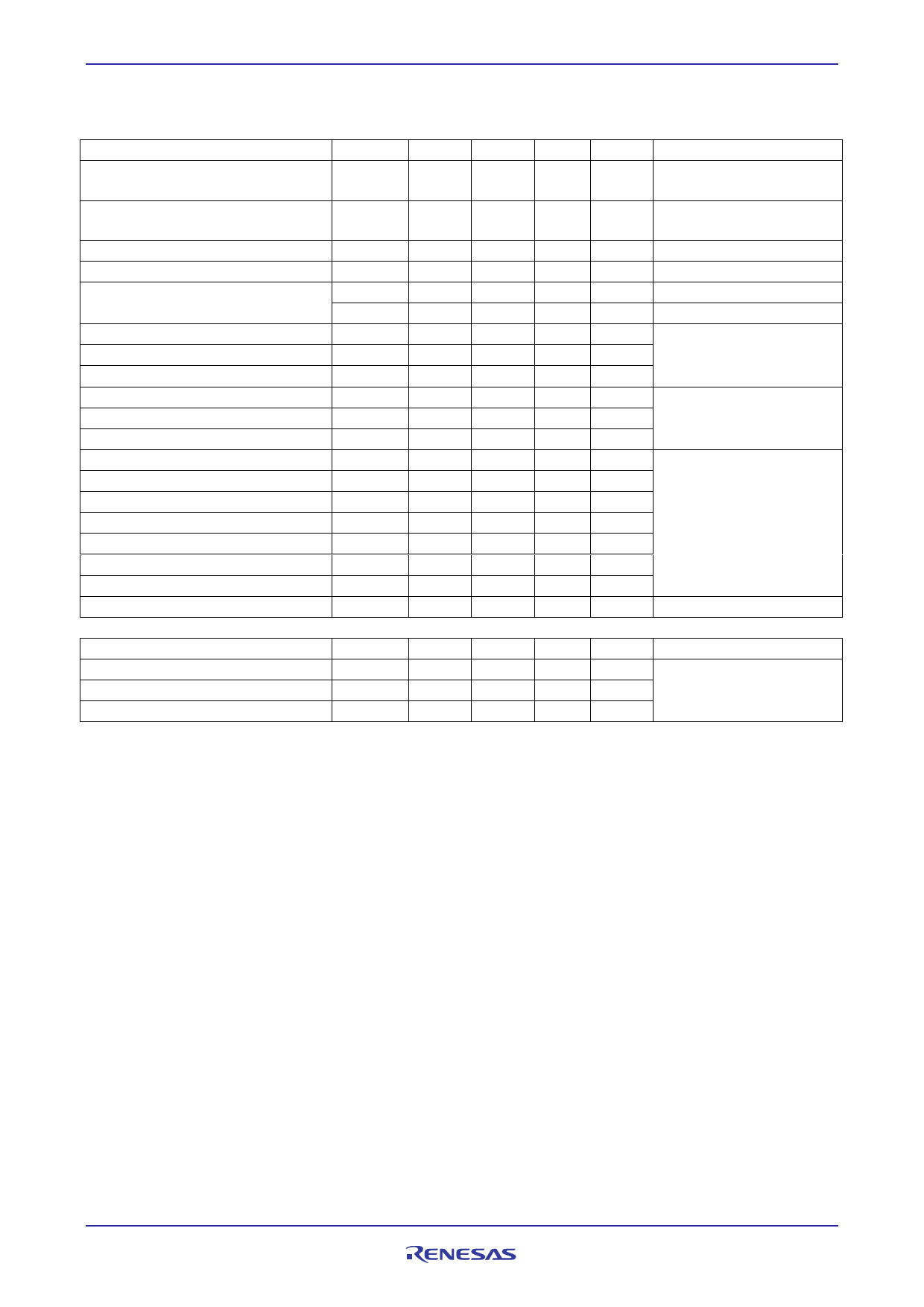
Item
Symbol Min
Zero gate voltage collector current
/ Diode reverse current
ICES / IR
—
Gate to emitter leak current
IGES
—
Gate to emitter cutoff voltage
VGE(off)
4.0
Collector to emitter saturation voltage VCE(sat)
—
VCE(sat)
—
Input capacitance
Cies
—
Output capacitance
Coes
—
Reveres transfer capacitance
Cres
—
Total gate charge
Qg
—
Gate to emitter charge
Qge
—
Gate to collector charge
Qgc
—
Switching time
td(on)
—
tr
—
td(off)
—
tf
—
(Ta = 25°C)
Typ Max Unit
Test Conditions
—
100
μA VCE = 600 V, VGE = 0
—
±1
—
6.0
1.6
2.2
1.8
—
900
—
50
—
30
—
35
—
7
—
20
—
40
—
45
—
60
—
100
—
μA VGE = ±30 V, VCE = 0
V
VCE = 10 V, IC = 1 mA
V
IC = 15 A, VGE = 15 V Note3
V
IC = 30A, VGE = 15 V Note3
pF VCE = 25 V
pF
VGE = 0
pF f = 1 MHz
nC VGE = 15 V
nC VCE = 300 V
nC IC = 15 A
ns IC = 15 A
ns RL = 20 Ω
ns
VGE = 15 V
ns Rg = 5 Ω
FRD Forward voltage
VF
—
1.8
2.3
V
IF = 15 A Note3
FRD reverse recovery time
trr
—
100
—
ns IF = 15 A
diF/dt = 100 A/μs
Notes: 3. Pulse test.
4. Under development — The specifications potentially be changed without notice.
REJ03G1844-0100 Rev.1.00 Oct 14, 2009
Page 2 of 3
Share Link: 