RD12MVP1(2006) データシートの表示(PDF) - Mitsumi
部品番号
コンポーネント説明
一致するリスト
RD12MVP1 Datasheet PDF : 7 Pages
| |||
ELECTROSTATIC SENSITIVE DEVICE
OBSERVE HANDLING PRECAUTIONS
MITSUBISHI RF POWER MOS FET
RD12MVP1
RoHS Compliance, Silicon MOSFET Power Transistor, 175MHz, 10W
DESCRIPTION
RD12MVP1 is a MOS FET type transistor
specifically designed for VHF RF power
amplifiers applications.
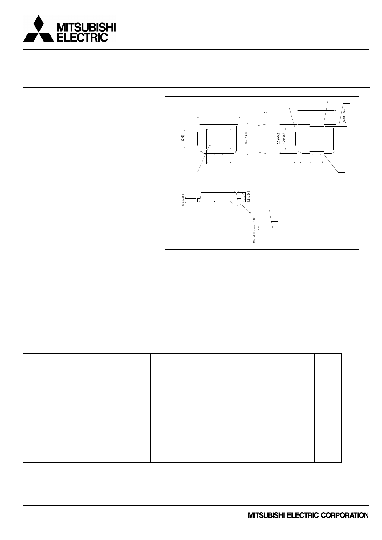
OUTLINE DRAWING
8.0+/-0.2
(d)
(b)
0.2+/-0.05
7.0+/-0.2
(a)
(b)
FEATURES
•High Power Gain
Pout>10W, Gp>13dB@Vdd=7.2V,f=175MHz
•High Efficiency: 55%min. (175MHz)
•No gate protection diode
APPLICATION
For output stage of high power amplifiers in
VHF band mobile radio sets.
INDEX MARK
[Gate]
(4.5)
0.95+/-0.2
2.6+/-0.2
TOP VIEW SIDE VIEW
DETAIL A
SIDE VIEW
DETAIL A
(c)
BOTTOM VIEW
Terminal No.
(a)Drain [output]
(b)Source [GND]
(c)Gate [input]
(d)Source
UNIT:mm
NOTES:
1. ( ) Typical value
RoHS COMPLIANT
RD12MVP1 is a RoHS compliant product.
RoHS compliance is indicating by the letter “G” after the Lot Marking. This product includes the lead in high
melting temperature type solders. However, it applicable to the following exceptions of RoHS Directions.
1.Lead in high melting temperature type solders (i.e. tin-lead older alloys containing more than85% lead.)
ABSOLUTE MAXIMUM RATINGS
(Tc=25°C, UNLESS OTHERWISE NOTED)
SYMBOL
PARAMETER
CONDITIONS
VDSS
Drain to Source Voltage VGS=0V
VGSS
Gate to Source Voltage VDS=0V
ID
Drain Current
Pin
Input Power
Zg=Zl=50Ω
Pch
Channel Dissipation
Tc=25°C
Tj
Junction Temperature
Tstg
Storage Temperature
Rthj-c Thermal Resistance
Junction to Case
Note: Above parameters are guaranteed independently.
RATINGS
60
-5 to +20
4.0
1.0
125
+150
-40 to +125
1.5
UNIT
V
V
A
W
W
°C
°C
°C/W
ELECTRICAL CHARACTERISTICS (Tc=25°C, UNLESS OTHERWISE NOTED)
SYMBOL
PARAMETER
CONDITIONS
LIMITS
MIN. TYP. MAX.
IDSS Zero Gate Voltage Drain Current VDS=17V, VGS=0V
-
-
10
IGSS Gate to Source Leak Current VGS=10V, VDS=0V
-
-
1.0
VTH Gate Threshold Voltage
VDS=12V, IDS=1mA
1.8
-
4.4
Pout Output Power
f=175MHz,VDD=7.2V
10
12
-
ηD Drain Efficiency
Pin=0.5W,Idq=1.0A
55
57
-
VDD=9.5V,Po=10W(Pin Control)
VSWRT Load VSWR tolerance
f=175MHz,Idq=1.0A,Zg=50Ω
Load VSWR=20:1(All Phase)
No destroy
Note: Above parameters, ratings, limits and conditions are subject to change.
UNIT
uA
uA
V
W
%
-
RD12MVP1
MITSUBISHI ELECTRIC
1/7
1st Jun. 2006
Share Link: 