R3115Z データシートの表示(PDF) - RICOH Co.,Ltd.
部品番号
コンポーネント説明
一致するリスト
R3115Z Datasheet PDF : 28 Pages
| |||
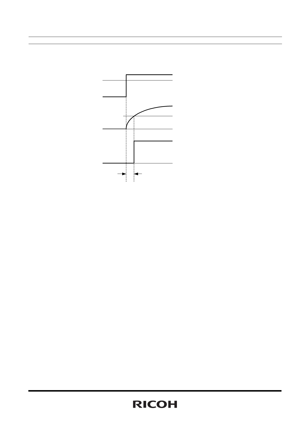
• Operation of Output Delay
Supply Voltage
Released Voltage +VDET
R3115Z
Capacitor Voltage
CD Pin Threshold Voltage (VTCD)
GND
Output Voltage
GND
Output Delay Time(tD)
When the supply voltage which is higher than released voltage is forced to VDD pin, charge to an external
capacitor starts, then capacitor voltage increases. Until the capacitor voltage reaches to CD Pin threshold voltage,
output voltage maintains “L”. When the capacitor voltage becomes higher than CD pin threshold voltage, output
voltage is reversed from "L” to "H". Where, the time interval between the rising edge of supply voltage and output
voltage reverse point means output delay time.
• Output Delay Time
Output Delay Time (tD) can be calculated with the next formula.
tD=0.69×RD×CD(s)
RD is internal resistor and set at 6.5MΩ(Typ.) typically. CD(F) describes the capacitance value of an external
capacitor. Therefore,
tD=0.69×6.5×106×CD(s)
9
Share Link: 