QT300 データシートの表示(PDF) - Quantum Research Group
部品番号
コンポーネント説明
一致するリスト
QT300 Datasheet PDF : 14 Pages
| |||
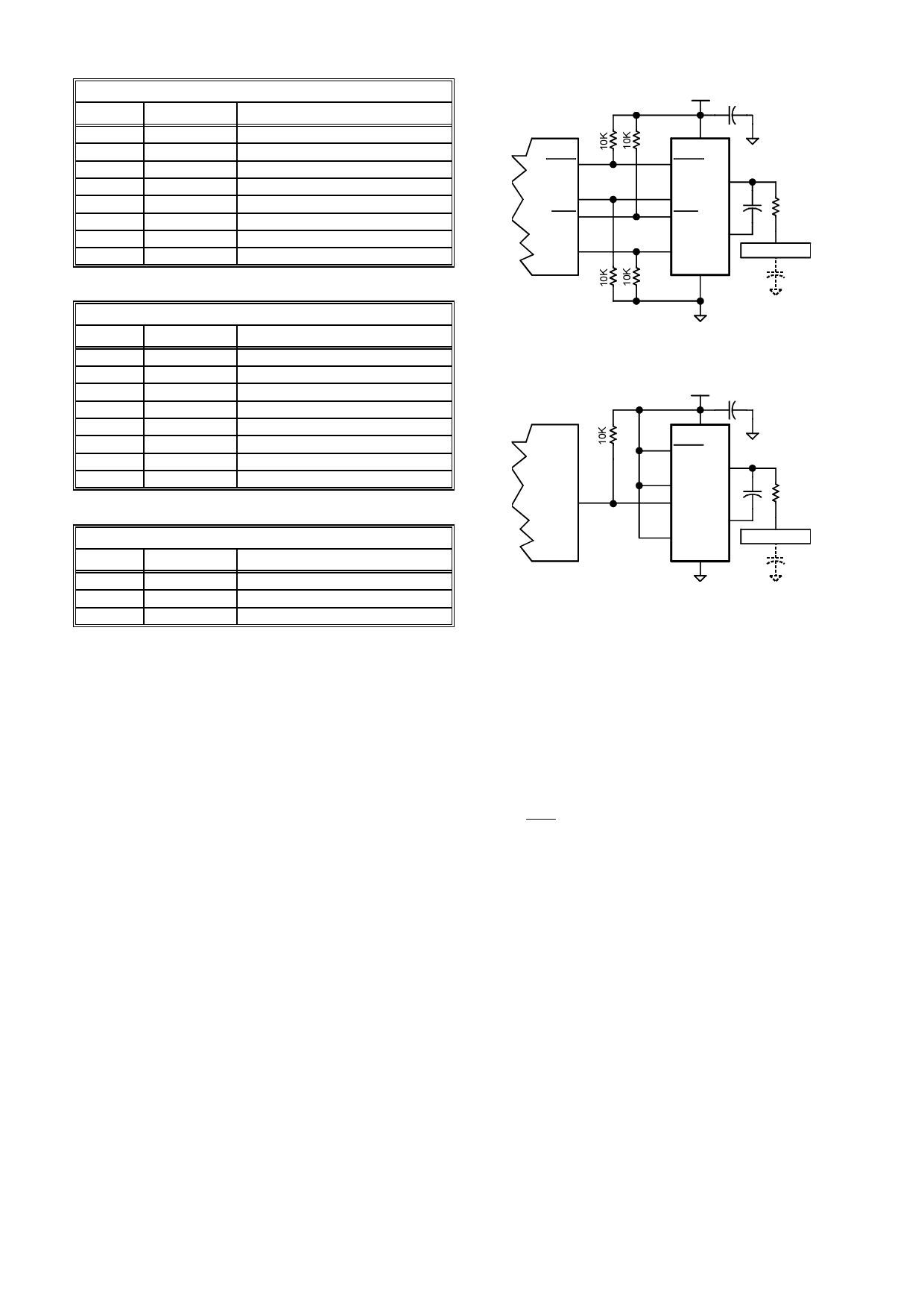
Table 1-1 SPI Mode Pin Description
Pin
Name
Function
1
/DRDY
Data Ready
2
SCK
Serial data clock
3
SNS1
Sense 1 line
4
VSS
Negative supply (ground)
5
SNS2
Sense 2 line
6
/REQ
Request input
7
SDO
Serial data out
8
VDD
Positive supply
HOST
MICRO
DRDY
SCK
REQ
SDI
Vdd
100nF
QT300 8
Vdd
1 DRDY
SNS1 3
2 SCK
6 REQ
SNS2 5
Rs
Cs
7 SDO
ELECTRODE
Vss
4
Cx
Table 1-2 1W UART Mode Pin Description
Pin
Name
Function
1
-
Connect to Vdd or Vss
2
-
Connect to Vdd or Vss
3
SNS1
Sense 1 line
4
VSS
Negative supply (ground)
5
SNS2
Sense 2 line
6
1W
1W UART Line
7
-
8
VDD
Connect to Vdd or Vss
Positive supply
Table 1-3 Alternate Cloning Pin Functions
Pin
Name
Function
2
SCK
6
SDI
Serial clone data clock
Serial clone data in
7
SDO
Serial clone data out
1 - OVERVIEW
The QT300 is a digital burst mode charge-transfer (QT)
capacitance-to-digital converter (CDC) designed for
applications requiring raw signal information such as fluid
level sensing and distance gauging; it outputs raw digital
signal data over a serial interface. The output data is in a
16-bit format; signal levels depend on load (Cx) and the
sampling capacitor value (Cs).
Sensitivity is a function of electrode size, shape, orientation,
the composition and aspect of the object being sensed, the
thickness and composition of any dielectric overlaying the
electrode, and the degree of mutual coupling between the
electrode and the object being sensed, in addition to the
electrical parameters Cs and Cx as described in Section 1.2
below.
1.1 Basic Operation
The QT300 does no internal signal processing; data is simply
returned via one of two serial port types.
There are two basic types of serial interface: 4-wire SPI and
a simple single wire (‘1W’) UART. The SPI interface allows
multiple devices to be connected on one SPI bus, while
the1W UART requires that the controller have one dedicated
pin for each QT300. There are two types of SPI mode,
master and slave.
Figure 1-1 Basic QT300 Circuit in SPI mode.
HOST
MICRO
1W UART
Vdd
100nF
QT300 8
Vdd
1 DRDY
SNS1 3
2 SCK
6 1W
SNS2 5
Rs
Cs
7 SDO
ELECTRODE
Vss
4
Cx
Figure 1-2 Basic QT300 Circuit in UART mode.
The type of serial port and its mode can be selected via the
cloning process using a QTM300CA programming adapter.
The QT300 operates only on request from a host device.
After initiation via a trigger signal, the QT300 generates an
acquisition burst and sends the resulting raw signal data
back via one of the serial modes.
1.2 Burst Length
The burst length (and hence the signal level and sensitivity)
is described by the following formula:
BL =
k$CS
CX
where Cs is the reference capacitor, Cx is the unknown load
capacitance (including internal pin and wiring capacitance)
and ‘k’ is a constant, typically 0.51, which varies very slightly
from device to device.
The device has an internal Cx, Csns, which adds to the Cx in
the formula. This capacitance is about 11pF.
Each doubling of Cs increases the signal level and
differential sensitivity by a factor of two. Likewise, doubling
Cx reduces the signal level and differential sensitivity by a
factor of two (Figures 7-4, 7-5, 7-7, 7-7, page 11).
The response can be linearized over a particular Cx range to
a great extent by making the delta-Cx of interest a small part
of the background level of Cx. If the delta Cx is 10pF on top
of 20pF, the response will be linear to 10% of full scale. But if
the desired delta-Cx range is 10pF on top of 100pF, the
LQ
2
QT300 R1.02/0204
Share Link: 