SL4034BN データシートの表示(PDF) - System Logic Semiconductor
部品番号
コンポーネント説明
一致するリスト
SL4034BN
System Logic Semiconductor

SL4034BN Datasheet PDF : 9 Pages
| |||
SL4034B
8-Stage Static Bidirectional Parallel/
Serial Input/Output Bus Register
High-Voltage Silicon-Gate CMOS
The SL4034B is a static eight-stage parallel-or serial-input parallel-
output register. It can be used to:
1) bidirectionally transfer parallel information between two buses, 2)
convert serial data to parallel form and direct the parallel data to either
of two buses, 3) store (recirculate) parallel data, or 4) accept parallel
data from either of two buses and convert that data to serial form.
Inputs that control the operations include a single-phase CLOCK (CL),
A DATA ENABLE (AE), ASYNCHRONOUS/SYNCHRONOUS (A/S),
A-BUS-TO-B-BUS/ B-BUS-TO-A-BUS (A/B), and PARALLEL/SERIAL
(P/S).
Data inputs include 16 bidirectional parallel data lines of which the
eight A data lines are inputs (3-state outputs) and the B data lines are
outputs (inputs) dependung on the signal level on the A/B input. In
addition, an input for SERIAL DATA is also provided.
All register stages are D-type master-slave flip-flops with
separate master and slave clock inputs generated internally to allow
synchronous or asynchronous data transfer from master to slave.
• Operating Voltage Range: 3.0 to 18 V
• Maximum input current of 1 µA at 18 V over full package-
temperature range; 100 nA at 18 V and 25°C
• Noise margin (over full package temperature range):
1.0 V min @ 5.0 V supply
2.0 V min @ 10.0 V supply
2.5 V min @ 15.0 V supply
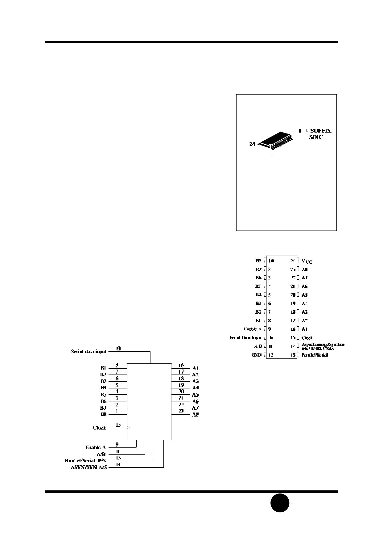
LOGIC DIAGRAM
ORDERING INFORMATION
SL4034BD SOIC
TA = -55° to 125° C
for package
PIN ASSIGNMENT
PIN 24=VCC
PIN 12= GND
SLS
System Logic
Semiconductor
Share Link: