SN74LS151DR2 データシートの表示(PDF) - ON Semiconductor
部品番号
コンポーネント説明
一致するリスト
SN74LS151DR2 Datasheet PDF : 8 Pages
| |||
SN74LS151
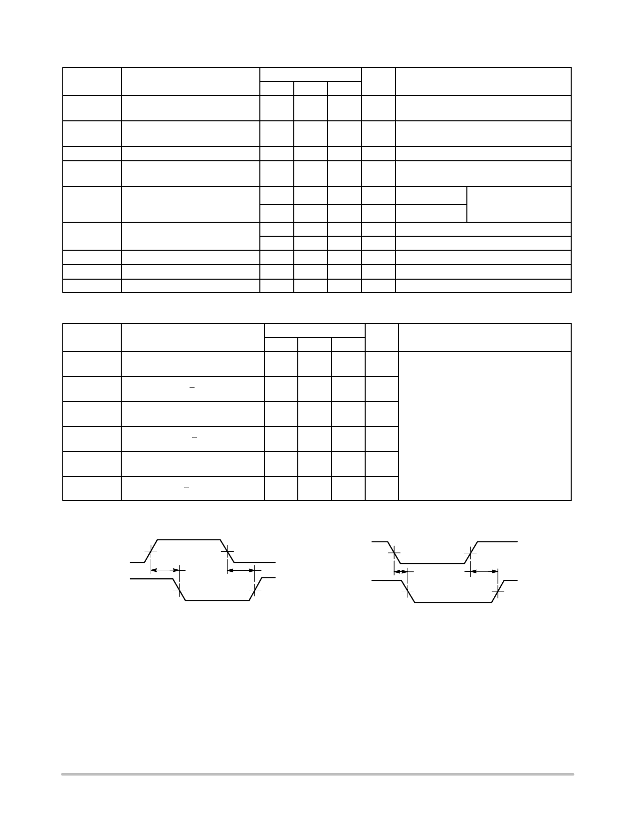
DC CHARACTERISTICS OVER OPERATING TEMPERATURE RANGE (unless otherwise specified)
Limits
Symbol
VIH
Parameter
Input HIGH Voltage
Min Typ Max Unit
Test Conditions
2.0
V
Guaranteed Input HIGH Voltage for
All Inputs
VIL
Input LOW Voltage
0.8
Guaranteed Input LOW Voltage for
V
All Inputs
VIK
VOH
Input Clamp Diode Voltage
Output HIGH Voltage
–0.65 –1.5
V
2.7
3.5
V
VOL
Output LOW Voltage
0.25 0.4
V
0.35 0.5
V
IIH
Input HIGH Current
20
µA
0.1
mA
IIL
Input LOW Current
–0.4 mA
IOS
Short Circuit Current (Note 2)
–20
–100 mA
ICC
Power Supply Current
10
mA
2. Not more than one output should be shorted at a time, nor for more than 1 second.
VCC = MIN, IIN = –18 mA
VCC = MIN, IOH = MAX, VIN = VIH
or VIL per Truth Table
IOL = 4.0 mA
IOL = 8.0 mA
VCC = VCC MIN,
VIN = VIL or VIH
per Truth Table
VCC = MAX, VIN = 2.7 V
VCC = MAX, VIN = 7.0 V
VCC = MAX, VIN = 0.4 V
VCC = MAX
VCC = MAX
AC CHARACTERISTICS (TA = 25°C)
Limits
Symbol
tPLH
tPHL
tPLH
tPHL
tPLH
tPHL
tPLH
tPHL
tPLH
tPHL
tPLH
tPHL
Parameter
Propagation Delay
Select to Output Z
Propagation Delay
Select to Output Z
Propagation Delay
Enable to Output Z
Propagation Delay
Enable to Output Z
Propagation Delay
Data to Output Z
Propagation Delay
Data to Output Z
Min Typ Max Unit
27
18
43
30
ns
14
23
20
32
ns
26
42
20
32
ns
15
24
18
30
ns
20
32
16
26
ns
13
21
12
20
ns
Test Conditions
VCC = 5.0 V
CL = 15 pF
AC WAVEFORMS
VIN
VOUT
1.3 V
tPHL
1.3 V
1.3 V
tPLH
1.3 V
Figure 1.
VIN
VOUT
1.3 V
tPHL tPLH
1.3 V
1.3 V
1.3 V
Figure 2.
http://onsemi.com
4
Share Link: 