LC863320 データシートの表示(PDF) - SANYO -> Panasonic
部品番号
コンポーネント説明
一致するリスト
LC863320 Datasheet PDF : 20 Pages
| |||
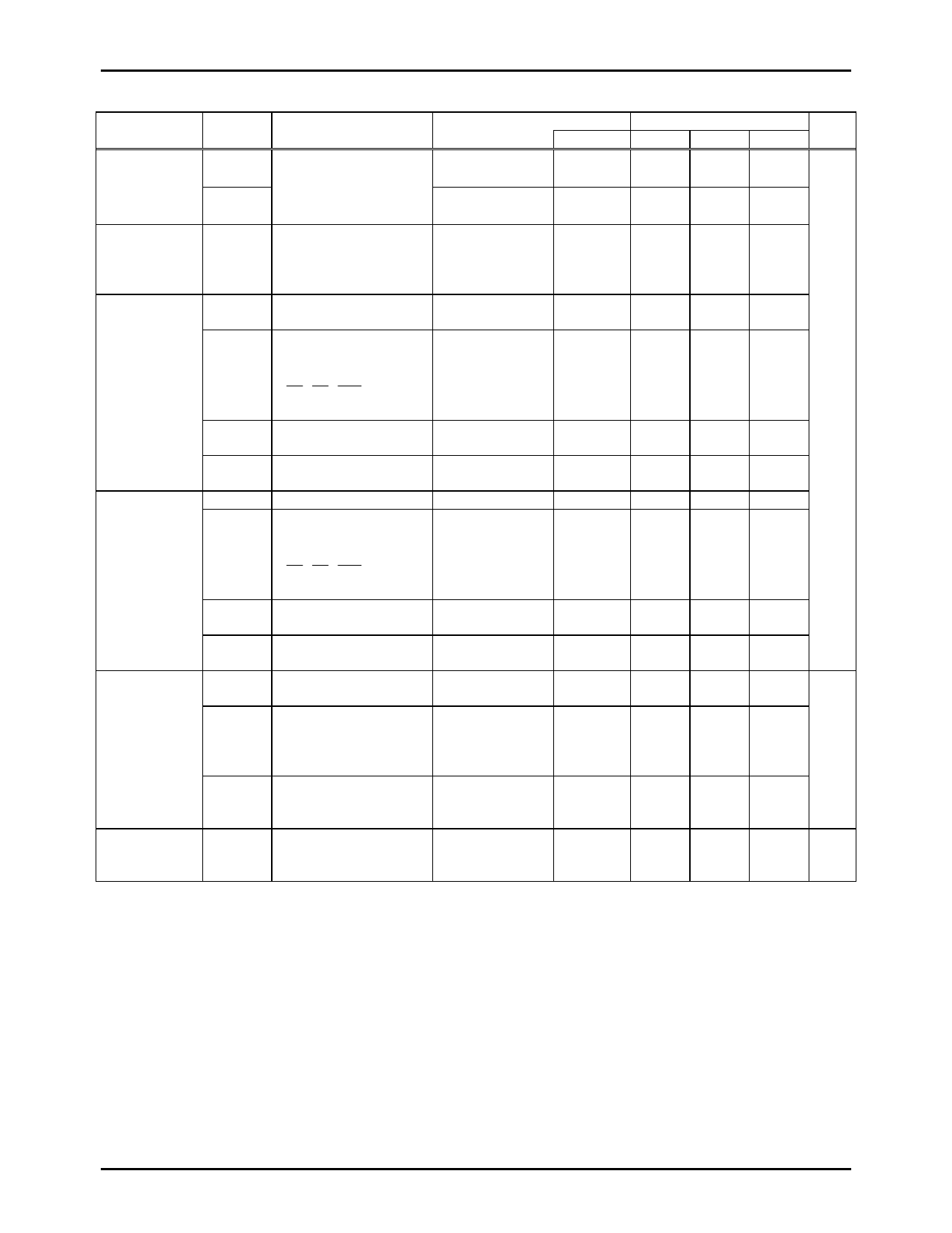
LC863332/28/24/20/16A
2. Recommended Operating Range at Ta= -10°C to +70°C, VSS=0V
Parameter Symbol
Pins
Operating
supply voltage
range
VDD(1)
VDD(2)
VDD
Hold voltage VHD VDD
High level
input voltage
Low level input
voltage
Operation
cycle time
VIH(1)
VIH(2)
VIH(3)
VIH(4)
VIL(1)
VIL(2)
VIL(3)
VIL(4)
tCYC(1)
tCYC(2)
Port 0 (Schumitt)
•Ports 1,6 (Schumitt)
•Port 7 (Schumitt)
port input/interrupt
• HS , VS , RES
(Schumitt)
Port 70
Watchdog timer input
•Port 8
port input
Port 0 (Schumitt)
•Ports 1,6 (Schumitt)
•Port 7 (Schumitt)
port input/interrupt
• HS , VS , RES
(Schumitt)
Port 70
Watchdog timer input
Port 8
port input
tCYC(3)
Oscillation
frequency
range
FmRC
Conditions
VDD[V]
Ratings
min. typ. max.
unit
0.844µs ≤ tCYC
≤ 0.852µs
4.5
5.5
V
4µs ≤ tCYC ≤
400µs
4.5
5.5
RAMs and the
2.0
5.5
registers data are
kept in HOLD
mode.
Output disable
4.5 - 5.5 0.6VDD
VDD
Output disable
4.5 - 5.5 0.75VDD
VDD
Output disable
Output disable
Output disable
Output disable
4.5 - 5.5 VDD-0.5
4.5 - 5.5 0.7VDD
4.5 - 5.5 VSS
4.5 - 5.5 VSS
VDD
VDD
0.2VDD
0.25VDD
Output disable
4.5 - 5.5 VSS
0.6VDD
Output disable
4.5 - 5.5 VSS
0.3VDD
•All functions
operating
•AD converter
operating
•OSD is not
operating
•OSD and AD
converter are not
operating
Internal RC
oscillation
4.5 - 5.5
4.5 - 5.5
4.5 - 5.5
4.5 - 5.5
0.844
0.844
0.844
0.4
0.848
0.8
0.852 µs
30
400
3.0 MHz
No.6695-10/20
Share Link: 