PI6C2409 データシートの表示(PDF) - Pericom Semiconductor
部品番号
コンポーネント説明
一致するリスト
PI6C2409 Datasheet PDF : 8 Pages
| |||
PI6C2409
Zero Delay Clock Buffer 1122334455667788990011223344556677889900112233445566778899001122112233445566778899001122334455667788990011223344556677889900112211223344556677889900112233445566778899001122334455667788990011221122334455667788990011223344556677889900112233445566778899001122112233445566778899001122
Zero Delay and Skew Control
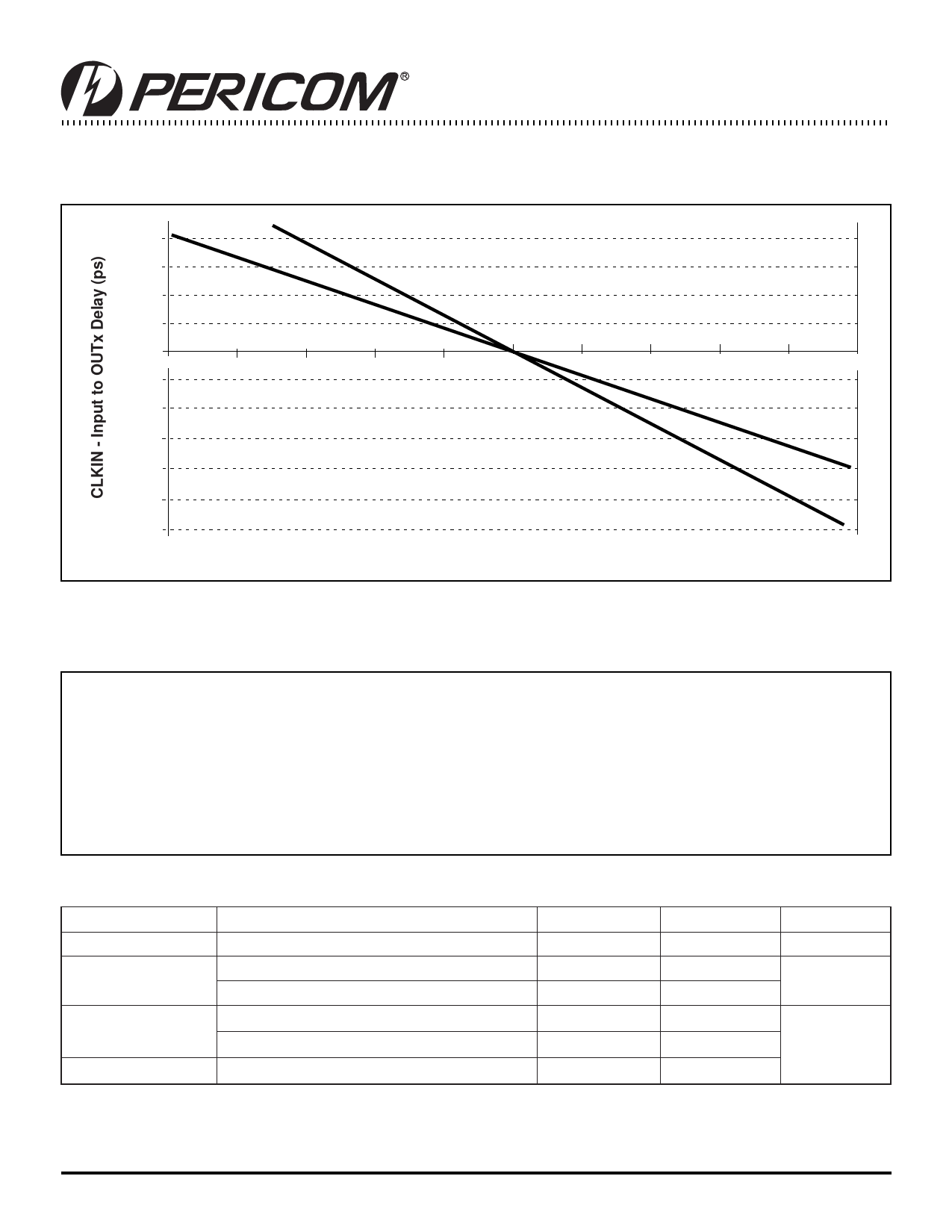
CLKIN Input to OUTx Delay vs. Difference in Loading between OUT0 pin and OUTx pins
800
600
400
200
0
-25
-20
-15
-10
-5
0
5
10
15
20
25
-200
-400
-600
PI6C2409-1H
-800
-900
PI6C2409-1
-1000
Output Load Difference: OUT0 Load - OUTx Load (pF)
The relationship between loading of the OUT0 signal and other outputs determines the input-output delay. Zero delay is achieved when
all outputs, including feedback, are loaded equally.
Maximum Ratings
Supply Voltage to Ground Potential ............................................................................................................................. –0.5Vto+7.0V
DC Input Voltage (Except CLKIN) ........................................................................................................................ –0.5VtoVDD+0.5V
DC Input Voltage CLKIN ...................................................................................................................................................... –0.5 to 7V
Storage Temperature ................................................................................................................................................... –65ºC to +150ºC
Maximum Soldering Temperature (10 seconds) ........................................................................................................................... 260ºC
Junction Temperature .................................................................................................................................................................. 150ºC
Static Discharge Voltage (per MIL-STD-883, Method 3015) .................................................................................................... >2000V
Operating Conditions (VCC = 3.3V ±0.3V)
Parameter
Description
VDD
Supply Voltage
Commerical Operating Temperature
TA
Industrial Operating Temperature
Load Capacitance, below 100 MHz
CL
Load Capacitance, from 100 MHz to 133 MHz
CIN
Input Capacitance
Min.
3.0
0
–40
Max.
3.6
70
85
30
15
7
Units
V
ºC
pF
3
PS8613A
07/15/03
Share Link: 