PI6C2405A-1HWIE(2010) データシートの表示(PDF) - Pericom Semiconductor
部品番号
コンポーネント説明
一致するリスト
PI6C2405A-1HWIE Datasheet PDF : 8 Pages
| |||
PI6C2405A
Zero Delay Clock Buffer
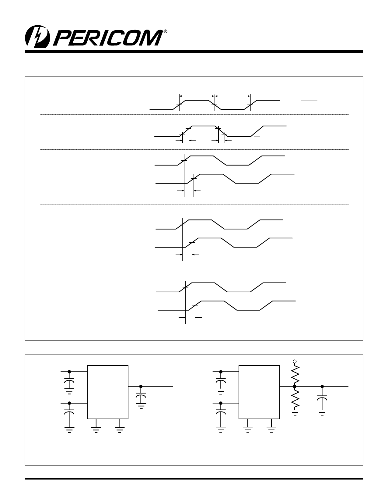
Switching Waveforms
Duty Cycle Timing
All Outputs Rise/Fall Time
Output-Output Skew
VDD/2
thigh
VDD/2
tlow
VDD/2
OUTPUT
2.0V
0.8V
tR
2.0V
0.8V
0V
tF
OUTPUT
OUTPUT
VDD/2
VDD/2
tSK(O)
tDC =
thigh
thigh+tlow
3.3V
Device-Device Skew
OUTPUT Device 1
VDD/2
OUTPUT Device 2
Input-Output Propagation Delay
INPUT
OUTPUT
VDD/2
VDD/2
tSK(D)
VDD/2
t0
0.1µF
0.1µF
Test Circuit 1
VDD
OUTPUTS
VDD
GND GND
CLK out
CLOAD
0.1µF
0.1µF
Test Circuit 2
VDD
OUTPUTS
VDD
GND GND
1kΩ
CLK out
1kΩ
10pF
Test Circuit for all parameters except tSLEW
Test Circuit for tSLEW ,Output slew rate on –1H device
11-0001
5
PS8592I
04/29/10
Share Link: 