PDI1394P25 データシートの表示(PDF) - Philips Electronics
部品番号
コンポーネント説明
一致するリスト
PDI1394P25 Datasheet PDF : 44 Pages
| |||
Philips Semiconductors
1-port 400 Mbps physical layer interface
Preliminary data
PDI1394P25
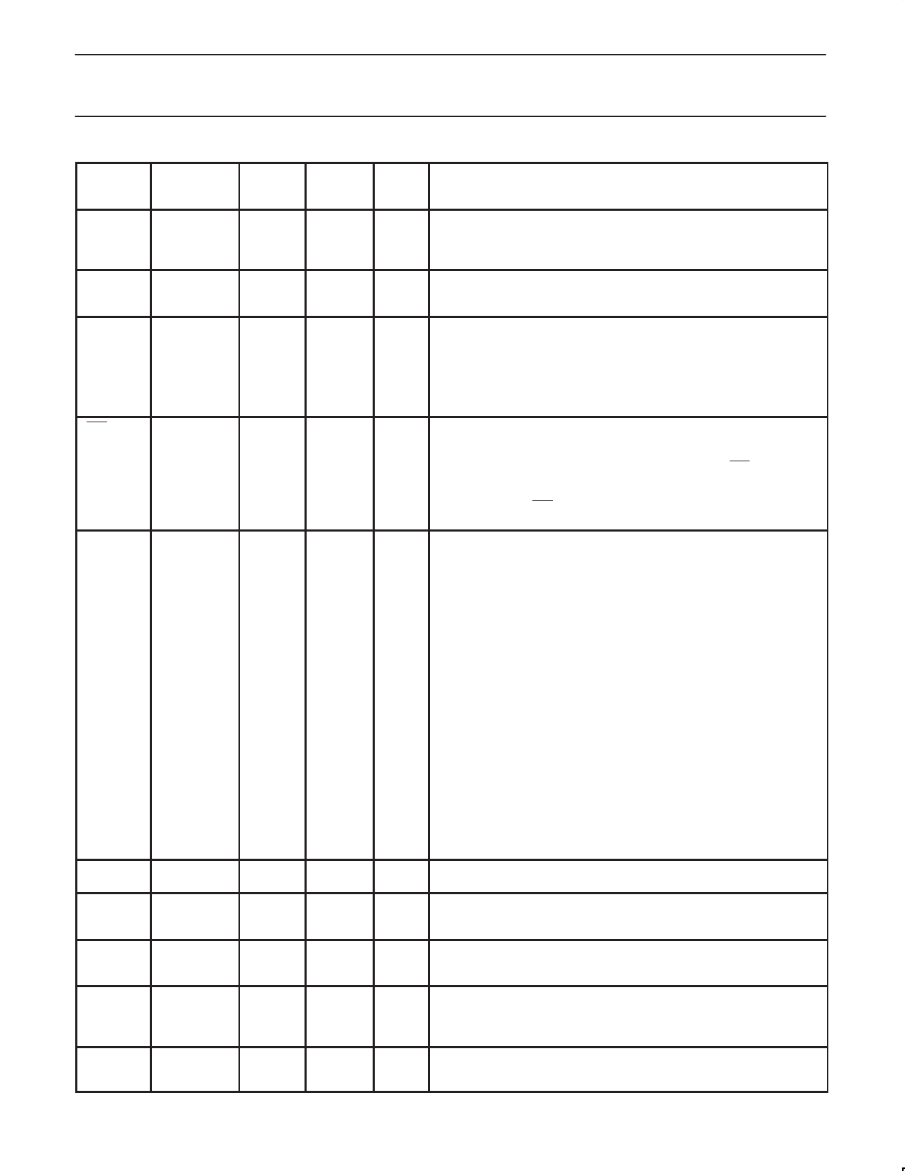
Name
D0–D7
DGND
DVDD
ISO
LPS
LREQ
NC
NC
PC0
PC1
PC2
PD
Pin Type
LQFP
LFBGA
I/O
Pin
Ball
Numbers Numbers
CMOS 5 V tol 6, 7, 8, H3, H4,
I/O
9, 10, 11, E4, H5,
12, 13
F4, G5,
F5, H6
Supply
17, 18, G1, G2,
—
63, 64
G7, G8,
H8
Supply
25, 26, D8, E6,
—
61, 62
F1, F2
CMOS
23
E8
I
CMOS 5 V tol 15
H7
I
CMOS 5 V tol 1
H1
I
No connect 54, 55
—
No connect 16, 43, A2, A3,
—
44, 45, B3, B4,
46, 47
C4
CMOS 5 V tol 20
F7
I
21
E7
22
F8
CMOS 5 V tol 14
G6
I
Description
Data I/Os. These are bi-directional data signals between the
PDI1394P25 and the LLC. Bus holders are built into these terminals.
Unused Dn pins should be pulled to ground through 10 kΩ resistors.
Digital circuit ground terminals. These terminals should be tied together
to the low impedance circuit board ground plane.
Digital circuit power terminals. A combination of high frequency
decoupling capacitors near each side of the IC package are suggested,
such as paralleled 0.1 µF and 0.001 µF. Lower frequency 10 µF filtering
capacitors are also recommended. These supply terminals are
separated from PLLVDD and AVDD internal to the device to provide noise
isolation. They should be tied at a low impedance point on the circuit
board.
Link interface isolation control input. This terminal controls the operation
of output differentiation logic on the CTL and D terminals. If an optional
isolation barrier of the type described in Annex J of IEEE Std 1394–1995
is implemented between the PDI1394P25 and LLC, the ISO terminal
should be tied low to enable the differentiation logic. If no isolation
barrier is implemented (direct connection), or bus holder isolation is
implemented, the ISO terminal should be tied high to disable the
differentiation logic.
Link Power Status input. This terminal is used to monitor the
active/power status of the link layer controller and to control the state of
the PHY-LLC interface. This terminal should be connected to either the
VDD supplying the LLC through a 10 kΩ resistor, or to a pulsed output
which is active when the LLC is powered. A pulsed signal should be
used when an isolation barrier exists between the LLC and PHY. (See
Figure 8)
The LPS input is considered inactive if it is sampled low by the PHY for
more than 2.6 µs (128 SYSCLK cycles), and is considered active
otherwise (i.e., asserted steady high or an oscillating signal with a low
time less than 2.6 µs). The LPS input must be high for at least 21 ns in
order to be guaranteed to be observed as high by the PHY.
When the PDI1394P25 detects that LPS is inactive, it will place the
PHY-LLC interface into a low-power reset state. In the reset state, the
CTL and D outputs are held in the logic zero state and the LREQ input is
ignored; however, the SYSCLK output remains active. If the LPS input
remains low for more than 26 µs (1280 SYSCLK cycles), the PHY-LLC
interface is put into a low-power disabled state in which the SYSCLK
output is also held inactive. The PHY-LLC interface is placed into the
disabled state upon hardware reset.
The LLC is considered active only if both the LPS input is active and the
LCtrl register bit is set to 1, and is considered inactive if either the LPS
input is inactive or the LCtrl register bit is cleared to 0.
LLC Request input. The LLC uses this input to initiate a service request
to the PDI1394P25. Bus holder is built into this terminal.
These pins are not internally connected and consequently are “don’t
cares”. Other vendors’ pin compatible chips may require
connections and external circuitry on these pins.
No connect.
Power Class programming inputs. On hardware reset, these inputs set
the default value of the power class indicated during self-ID.
Programming is done by tying the terminals high or low. Refer to
Table 21 for encoding.
Power Down input. A logic high on this terminal turns off all internal
circuitry except the cable-active monitor circuits which control the CNA
output. For more information, refer to Section 17.2
2001 Sep 06
6
Share Link: 