PCK2023DL データシートの表示(PDF) - Philips Electronics
部品番号
コンポーネント説明
一致するリスト
PCK2023DL
Philips Electronics

PCK2023DL Datasheet PDF : 30 Pages
| |||
Philips Semiconductors
CK408 (66/100/133/200 MHz) spread
spectrum differential system clock generator
Product data
PCK2023
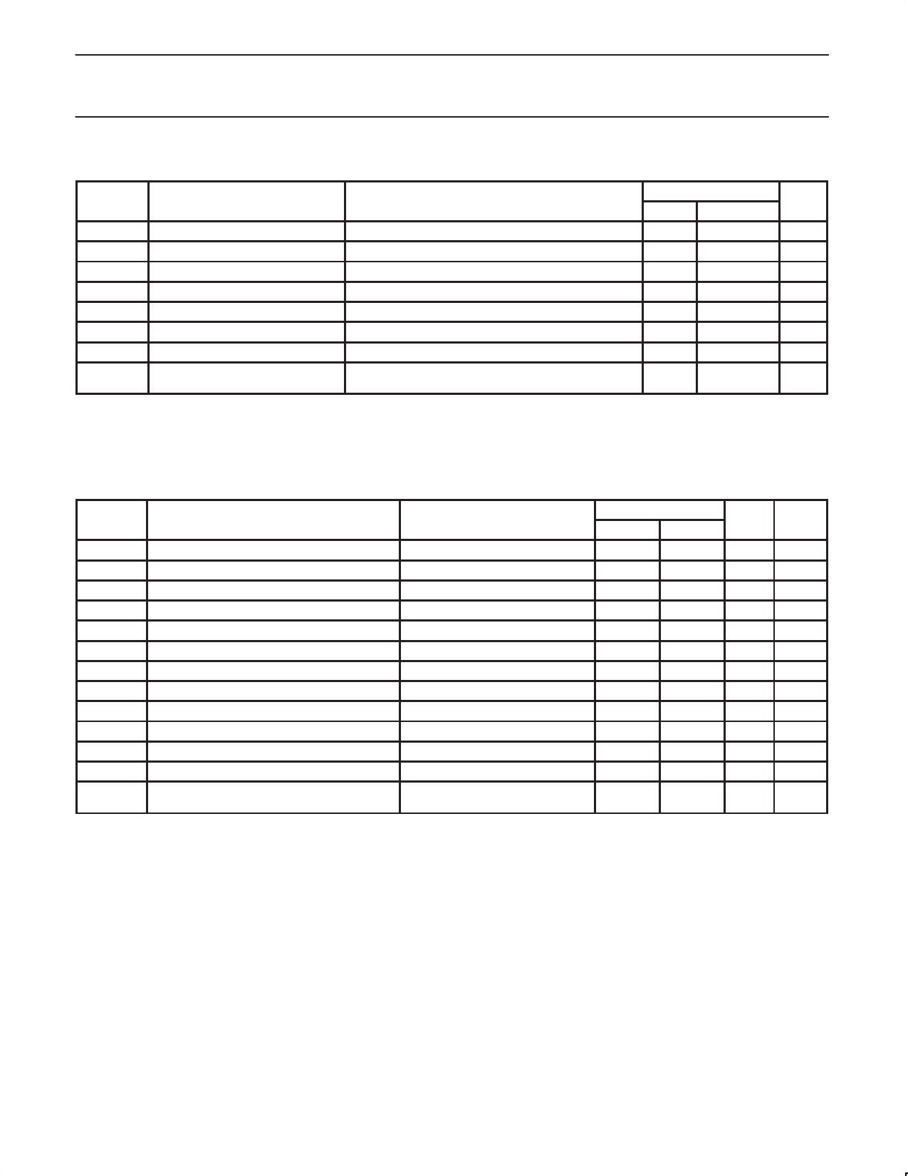
ABSOLUTE MAXIMUM RATINGS1, 2
SYMBOL
PARAMETER
CONDITION
LIMITS
MIN
MAX
UNIT
VDD3
DC 3.3 V supply
–0.5
+4.6
V
IIK
DC input diode current
VI < 0
—
–50
mA
VI
DC input voltage
Note 2
—
—
V
IOK
DC output diode current
VO > VDD or VO < 0
—
±50
mA
VO
DC output voltage
Note 2
–0.5
VDD + 0.5
V
IO
DC output source or sink current
VO = 0 to VDD
—
±50
mA
Tstg
Storage temperature range
–65
+150
°C
Ptot
Power dissipation per package
plastic medium-shrink (SSOP)
For temperature range: –40 to +125°C
above +55°C derate linearly with 11.3 mW/K
—
850
mW
NOTES:
1. Stresses beyond those listed may cause permanent damage to the device. These are stress ratings only and functional operation of the
device at these or any other conditions beyond those indicated under “Recommended Operating Conditions” is not implied. Exposure to
absolute-maximum-rated conditions for extended periods may affect device reliability.
2. The input and output voltage ratings may be exceeded if the input and output current ratings are observed.
DC OPERATING CONDITIONS
SYMBOL
PARAMETER
CONDITIONS
VDD3
DC 3.3 V supply voltage
AVDD
DC 3.3 V analog supply voltage
VIH
3.3 V input high voltage
VIL
3.3 V input high voltage
VOL3
3.3 V input low voltage
IOL = 1.0 mA
VOH3
3.3 V input high voltage
IOH = 1.0 mA
IIL
Input leakage current
0 < VIN < VDD
fref
reference frequency, oscillator normal value
CIN
Input pin capacitance
CXTAL
Xtal pin capacitance
COUT
Output pin capacitance
LPIN
Pin inductance
Tamb
Operating ambient temperature range in free
air
NOTES:
1. Input leakage current does not include inputs with pull up or pull down resistors.
2. This is a recommendation, not an absolute requirement.
3. As seen by the crystal. Device is intended to be used with a 17–20 pF AT crystal.
LIMITS
MIN
MAX
3.135
3.465
3.135
3.465
2.0
VSS – 0.3
—
VDD + 0.3
0.8
0.4
2.4
—
–5
+5
14.31818 14.31818
—
5
13.5
22.5
—
6
—
7
UNIT
V
V
V
V
V
V
µA
MHz
pF
pF
pF
nH
NOTES
1
2
3
2
2
0
+70
°C
2001 Sep 07
6
Share Link: