PCK2022RA データシートの表示(PDF) - Philips Electronics
部品番号
コンポーネント説明
一致するリスト
PCK2022RA Datasheet PDF : 14 Pages
| |||
Philips Semiconductors
CK00 (100/133 MHz) spread spectrum differential
system clock generator
Product data
PCK2022RA
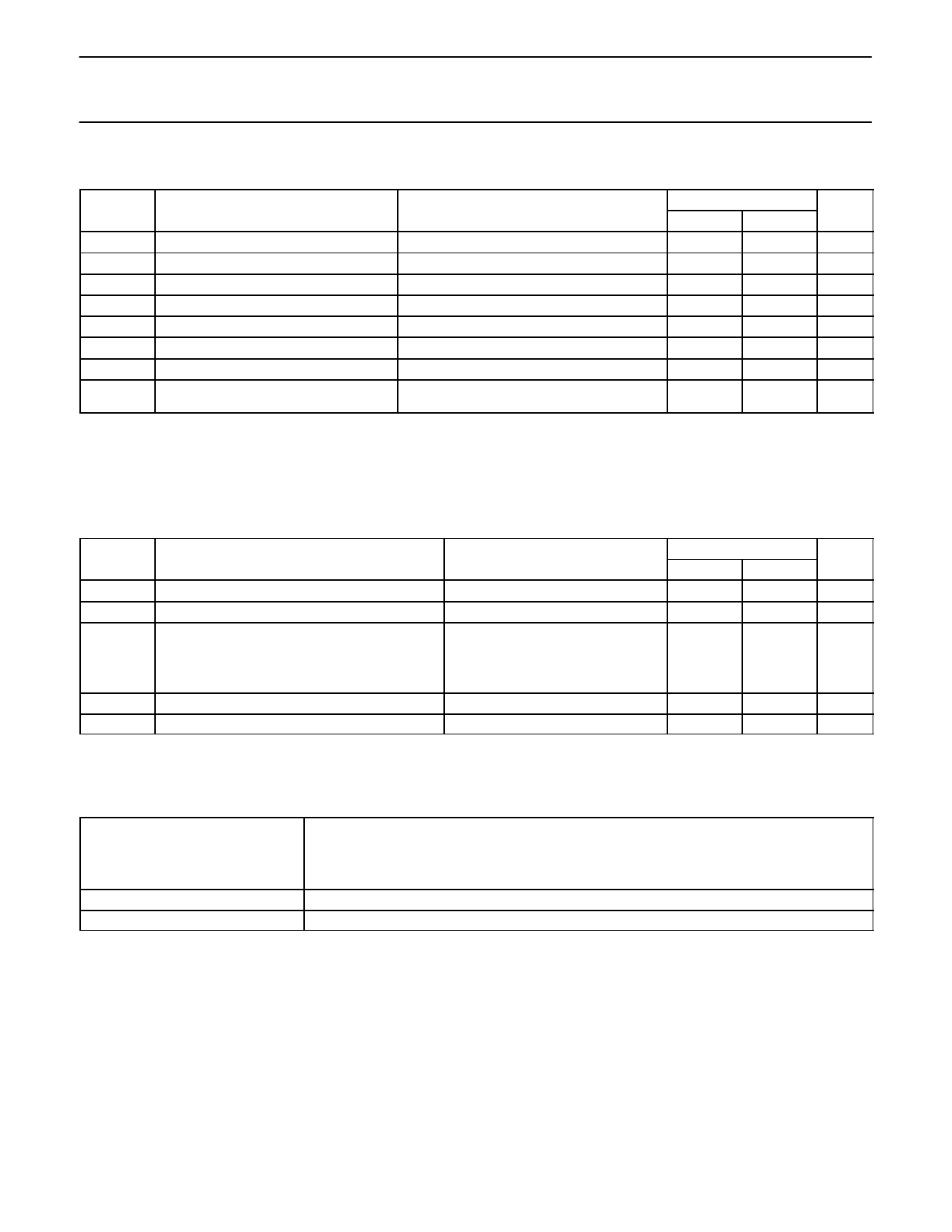
ABSOLUTE MAXIMUM RATINGS
SYMBOL
PARAMETER
CONDITIONS
LIMITS
MIN
MAX
UNIT
VDD3
DC 3.3 V supply
-0.5
4.6
V
IIK
DC input diode current
VI < 0
—
-50
mA
VI
DC input voltage
Note 2
-0.5
VDD
V
IOK
DC output diode current
VO > VDD or VO < 0
—
±50
mA
VO
DC output voltage
Note 2
-0.5
VDD+0.5
V
IO
DC output source or sink current
VO = 0 to VDD
—
±50
mA
Tstg
Storage temperature range
-65
+150
°C
Ptot
Power dissipation per package
plastic medium-shrink (SSOP)
For temperature range -40°C to +125°C;
—
above +55°C derate linearly with 11.3 mW/K
850
mW
NOTES:
1. Stresses beyond those listed may cause permanent damage to the device. These are stress ratings only and functional operation of the
device at these or any other condition beyond those indicated under “recommended operating condition” is not implied. Exposure to
absolute-maximum-rated conditions for extended periods may affect device reliability.
2. The input and output voltage rating may be exceeded if the input and output current ratings are observed.
RECOMMENDED OPERATING CONDITIONS
SYMBOL
PARAMETER
CONDITIONS
VDD3
AVDD
CL
DC 3.3 V supply voltage1
DC 3.3 V analog supply voltage1
Capacitive load on:
IOCLK
48 MHz clock
REF
Must meet IOCLK 2.1 requirements
1 device load
1 device load
fref
Reference frequency, oscillator normal value
Tamb
Operating ambient temperature range in free air
NOTE:
1. Supply voltage needs to be less than 20 mV before powering on to ensure proper PLL start-up.
LIMITS
MIN
MAX
3.135
3.465
3.135
3.465
10
10
10
14.31818
0
30
20
20
14.31818
+70
UNIT
V
V
pF
pF
pF
MHz
°C
POWER MANAGEMENT
CONDITION
Power-down mode (PWRDWN = 0)
Full active 100/133 MHz
MAXIMUM 3.3 V SUPPLY CONSUMPTION
MAXIMUM DISCRETE CAPACITANCE LOADS
VDDL = 3.465 V
ALL STATIC INPUTS = VDD3 OR VSS
60 mA
250 mA
2003 Jul 31
6
Share Link: 