PCK2010DL データシートの表示(PDF) - Philips Electronics
部品番号
コンポーネント説明
一致するリスト
PCK2010DL Datasheet PDF : 16 Pages
| |||
Philips Semiconductors
CK98 (100/133MHz) Spread Spectrum System Clock
Generator
Preliminary specification
PCK2010
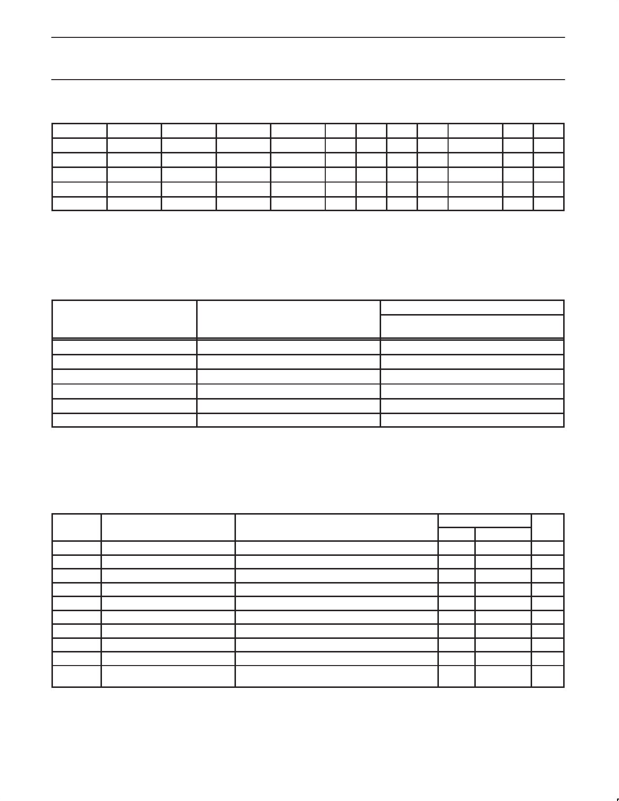
CLOCK ENABLE CONFIGURATION
CPUSTOP PWRDWN PCISTOP CPUCLK CPUDIV2 APIC 3V66 PCI PCIF REF 48MHz OSC VCOs
X
0
X
LOW
LOW
LOW LOW LOW LOW
LOW
OFF OFF
0
1
0
LOW
ON
ON LOW LOW ON
ON
ON ON
0
1
1
LOW
ON
ON LOW ON ON
ON
ON ON
1
1
0
ON
ON
ON ON LOW ON
ON
ON ON
1
1
1
ON
ON
ON ON ON ON
ON
ON ON
NOTES:
1. LOW means outputs held static LOW as per latency requirement below
2. ON means active.
3. PWRDWN pulled LOW, impacts all outputs including REF and 48MHz outputs.
4. All 3V66 clocks as well as CPU clocks should stop cleanly when CPUSTOP is pulled LOW.
5. CPUDIV2, IOAPIC, REF, 48MHz signals are not controlled by the CPUSTOP functionality and are enabled all in all conditions except when
PWRDWN is LOW.
POWER MANAGEMENT REQUIREMENTS
SIGNAL
SIGNAL STATE
LATENCY
NO. OF RISING EDGES OF FREE RUNNING
PCICLK
CPUSTOP
PCISTOP
PWRDWN
0 (DISABLED)
1 (ENABLED)
0 (DISABLED)
1 (ENABLED)
1 (NORMAL OPERATION)
0 (POWER DOWN)
1
1
1
1
3ms
2 MAX
NOTES:
1. Clock ON/OFF latency is defined as the number of rising edges of free running PCICLKs between the clock disable goes HIGH/LOW to the
first valid clock that comes out of the device.
2. Power up latency is when PWRDWN goes inactive (HIGH) to when the first valid clocks are driven from the device.
ABSOLUTE MAXIMUM RATINGS1, 2
In accordance with the Absolute Maximum Rating System (IEC 134)
Voltages are referenced to VSS (VSS = 0V)
SYMBOL
PARAMETER
CONDITION
VDD3
VDDQ3
VDDQ2
IIK
VI
IOK
VO
IO
TSTG
PTOT
DC 3.3V core supply voltage
DC 3.3V I/O supply voltage
DC 2.5V I/O supply voltage
DC input diode current
DC input voltage
DC output diode current
DC output voltage
DC output source or sink current
Storage temperature range
Power dissipation per package
plastic medium-shrink (SSOP)
VI < 0
Note 2
VO > VCC or VO < 0
Note 2
VO = 0 to VCC
For temperature range: –40 to +125°C
above +55°C derate linearly with 11.3mW/K
LIMITS
MIN
MAX
–0.5
+4.6
–0.5
+4.6
–0.5
+3.6
–50
–0.5
5.5
±50
–0.5
VCC + 0.5
±50
–65
+150
850
UNIT
V
V
V
mA
V
mA
V
mA
°C
mW
NOTES:
1. Stresses beyond those listed may cause permanent damage to the device. These are stress ratings only and functional operation of the
device at these or any other conditions beyond those indicated under “recommended operating conditions” is not implied. Exposure to
absolute-maximum-rated conditions for extended periods may affect device reliability.
2. The input and output voltage ratings may be exceeded if the input and output current ratings are observed.
1999 Mar 01
6
Share Link: 