PBL3853N データシートの表示(PDF) - Ericsson
部品番号
コンポーネント説明
一致するリスト
PBL3853N Datasheet PDF : 16 Pages
| |||
PBL 3853
Making any of the impedances unne-
cessary high will make the circuit sen-
sitive to RFI. All values given here are
approximate and serve as starting enti-
ties only. The final trimming of side tone
network is a cut and try proposition
because a part of the balance lies in the
acoustical path between the microphone
and earphone.
DC-Supply
In general
The most significant feature of this
speech circuit is its ability to draw
current from the line, that is used to a
DC-supply for auxiliary electronics and
for the receiver amplifier on the chip,
under maintaining the line impedance.
This function is boosted by two external
high β PNP transistors T1 and T2, and
internal amplifier and a comparator.
In detail
The circuit is designed such that it
supplies current first into the DC supply
output (priority) so that the micro-
computer which is controlling the auxi-
liary circuits and functions will have
power. The rest of the line current is
going to the speech function supply at
pin 4 (≈0.3mA) and through the transmit-
ter. The speech function needs 4mA
min. to operate to full specification. The
current to the DC supply is set by
expression:
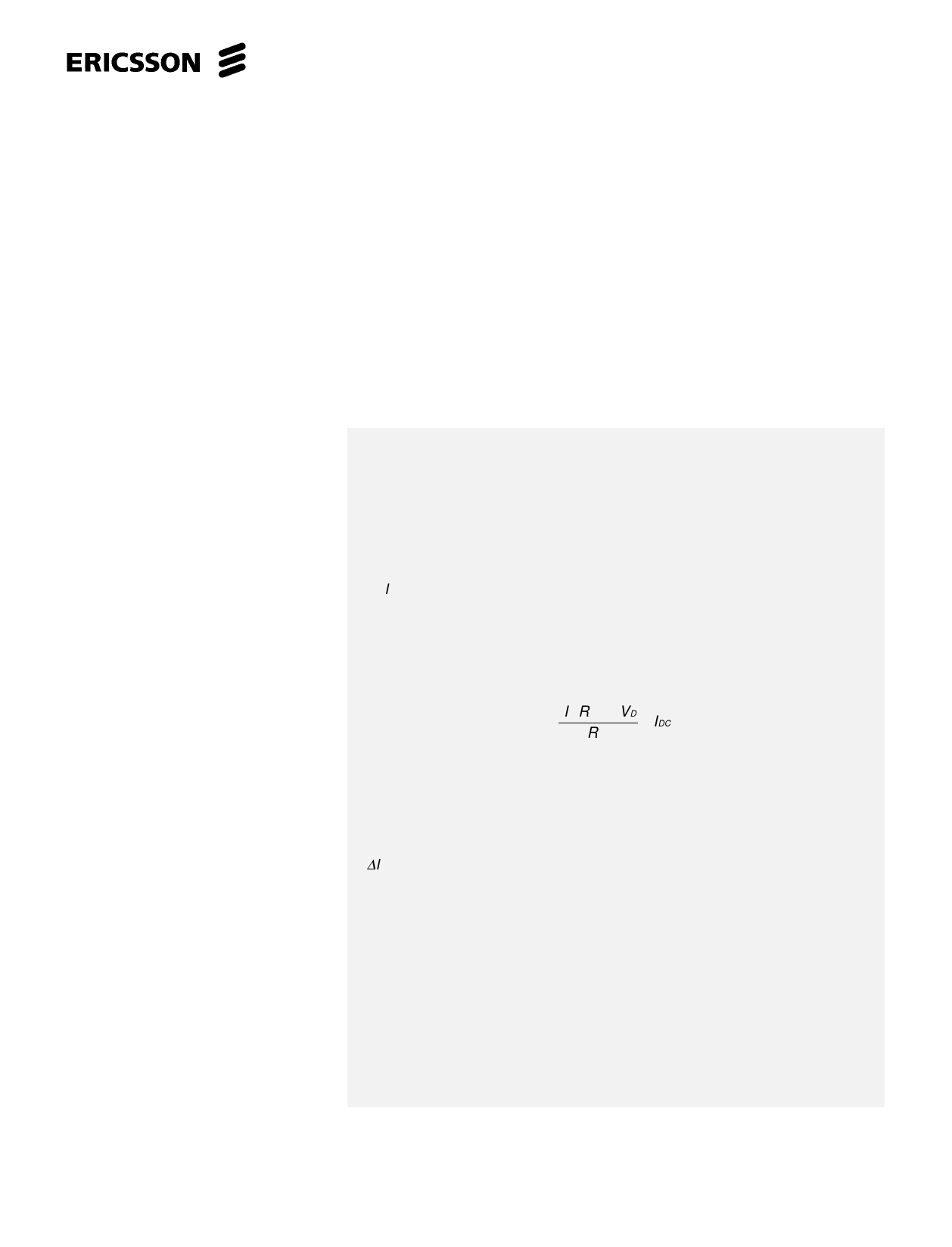
IDC = (I1 x R12 + VD)/R13 where VD
= 0.65V, I1 ≈ 4 - 0.3 = 3.7mA and
controlled with an amplifier through the
voltage between terminals 1 and 9. A
certain increase in the voltage (∆VL)
across the resistor R12 will result in an
equal increase in the voltage across R13
which gives the expression:
∆IL=∆I1 (1 + R12/R13). From this can be
seen that an increasing line current will
also partly increase the DC-supply
current.
The comparator will compare the
voltage at terminal 18 plus 2xVD
(≈ 1.3V), with the voltage at terminal 1,
whether it is higher or lower. The line
current will be distributed as follows: The
comparator will route the line current to
the DC-supply until the set current is
reached after which the exceeding line
current will be divided between the
transmitter and the DC-supply according
to the expression
∆IL = ∆I1 (1 + R12/R13).
Note: That the DC-supply charge current
coming from the line, given by the
expression VD/R13, because of
the constant voltage difference of
VD between the pins 1 and 9,
makes it possible to use the DC-
supply for external electronics at
low line currents even before the
speech function. It can be seen in
the figure 16 that the line voltage
at low line currents is given by
VL = V18 + 2 VD + I1xR12 ≈ 6.0V.
(V18 = 4.5V;I1 small)
The DC-supply level is monitored by a
circuit that will cut the charge current
whenever the line voltage with the
modulated signal reaches a value 2 x
diode drops below the DC level. The
current will be returned via TR2 to
ground thus maintaining the correct
impedance towards the line and making
it possible to transmit a swing to the line
that has lower level than the DC. See
figure 18. When the line voltage without
signal reaches the TR2 monitor level the
charge to the DC-supply will be cut off
whereby the receiver dies because it
draws its current from the DC-supply. In
case that the dc-characteristic is set
such that the current will come first to
the minimum working level (≈IDC + 4 mA)
then the transmitter will die first because
of the IDC priority.
Example:
A payphone is to be designed. According to the specification the minimum line
current is 20mA at 6V inclusive the bridge for the phone to work with all its auxiliary
functions. The auxiliary functions will need as much current as it is possible to draw
from the line and the worst case is naturally at the longest line length. The speech
section of the circuit with the earphone amplifier needs ≈ 4mA for function. In this
case the highest possible IDC with the longest line will be 20 - 4 = 16mA.
IL= I1 +Ipin4 +IDC , see figure 16
or
I1= IL - Ipin4 - IDC
or
IDC= IL - Ipin4 - I1
and
I1 R12 + VD= IDC R13
Values for R12 and R13:
( ) I1 ⋅ R 12 + VD = IDC
R 13
The speech function current consists of two branches I1 and the current to pin 4
which is ≈ 0.3mA thus the current I1 through R12 will be 4 - 0.3 = 3.7mA. VD is
taken to be 0.650V. Choose R12 = 50 Ω to start with. The voltage drop across this
resistor is translated to voltage drop across R13 which in its turn will steal available
voltage from VDC. These values render a R13 = 51.6 Ω.
An increasing available line current will be divided between I1 and IDC as follows:
∆I1 R12= ∆IDC R13
∆IL = ∆I1 + ∆IDC
∆I1 = ∆IL /( 1 + R12/R13 )
or
∆LDC = ∆IL /( 1 + R13/R12 )
∆IL= ∆I1(1+R12/R13)=∆IDC(1+R13/R12)
Simply, when the voltage drop across R13 reaches one diode drop (0.650V) then
the current will be divided between I1 and IDC as
1:(R13/R12) = 1:(51.6/50) ≈ 1:1.
11
Share Link: 