P4C164L-100P3C データシートの表示(PDF) - Semiconductor Corporation
部品番号
コンポーネント説明
一致するリスト
P4C164L-100P3C Datasheet PDF : 11 Pages
| |||
P4C164L
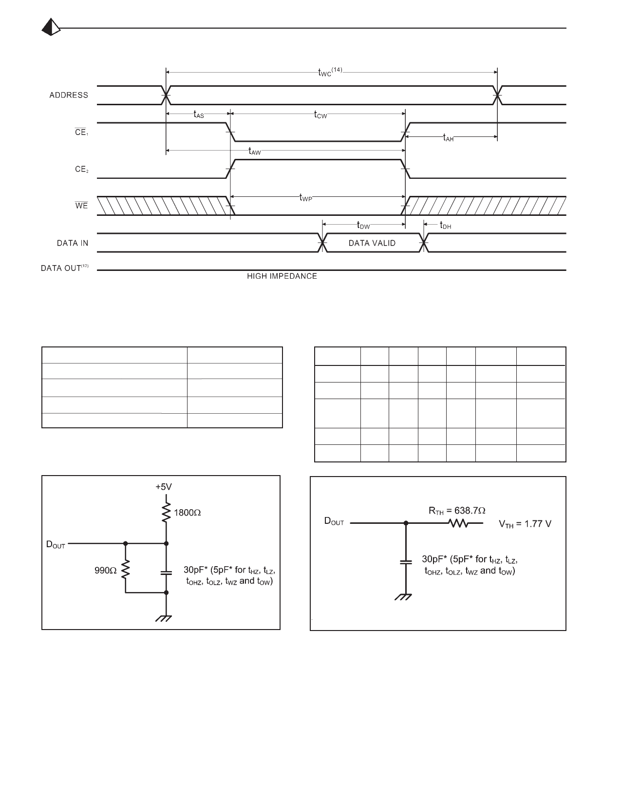
TIMING WAVEFORM OF WRITE CYCLE NO.2 (CE CONTROLLED)(6)
AC TEST CONDITIONS
Input Pulse Levels
Input Rise and Fall Times
GND to 3.0V
3ns
Input Timing Reference Level
1.5V
Output Timing Reference Level
1.5V
Output Load
See Figures 1 and 2
TRUTH TABLE
Mode
CE
1
CE2
OE
WE
I/O
Power
Standby H X X X High Z Standby
Standby X L X X High Z Standby
D
OUT
Disabled L
HH
H High Z Active
Read
Write
L
H
L
H DOUT Active
L H X L High Z Active
Figure 1. Output Load
* including scope and test fixture.
Note:
Because of the high speed of the P4C164L, care must be taken when
testing this device; an inadequate setup can cause a normal
functioning part to be rejected as faulty. Long high-inductance leads
that cause supply bounce must be avoided by bringing the VCC and
ground planes directly up to the contactor fingers. A 0.01 µF high
frequency capacitor is also required between VCC and ground.
Figure 2. Thevenin Equivalent
To avoid signal reflections, proper termination must be used; for
example, a 50Ω test environment should be terminated into a 50Ω load
with 1.77V (Thevenin Voltage) at the comparator input, and a 589Ω
resistor must be used in series with DOUT to match 639Ω (Thevenin
Resistance).
Document # SRAM116 REV B
Page 6 of 11
Share Link: 