MC14499DW データシートの表示(PDF) - Motorola => Freescale
部品番号
コンポーネント説明
一致するリスト
MC14499DW Datasheet PDF : 8 Pages
| |||
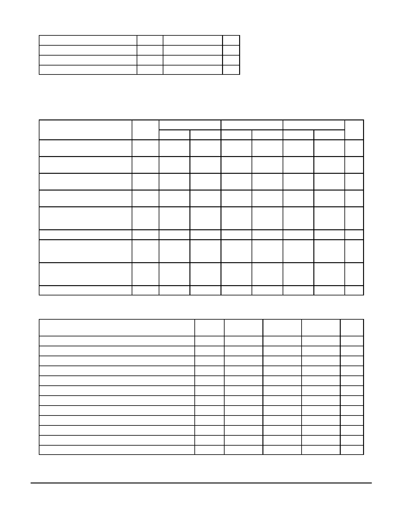
ÁÁÁÁÁÁÁÁÁÁÁÁÁÁÁÁÁÁÁÁÁÁÁÁÁÁÁÁÁÁÁÁÁÁÁÁÁÁÁÁÁÁÁÁ MAXIMUM RATINGS* (Voltages referenced to VSS)
ÁÁÁÁÁÁÁÁÁÁÁÁÁÁÁÁÁÁÁÁÁÁ Rating
Symbol
Value
Unit
ÁÁÁÁÁÁÁÁÁÁÁÁÁÁÁÁÁÁÁÁÁÁ DC Supply Voltage
VDD
– 0.5 to + 7
V
ÁÁÁÁÁÁÁÁÁÁÁÁÁÁÁÁÁÁÁÁÁÁ Input Voltage, All Inputs
Vin
– 0.5 to VDD + 0.5
V
ÁÁÁÁÁÁÁÁÁÁÁÁÁÁÁÁÁÁÁÁÁÁ Storage Temperature Range
Tstg
– 65 to + 150
°C
ÁÁÁÁÁÁÁÁÁÁÁÁÁÁÁÁÁÁÁÁÁÁ * Maximum Ratings are those values beyond which damage to the device may occur.
Functional operation should be restricted to the limits in the Electrical Characteristics table
or Circuit Operation section.
This device contains circuitry to protect the
inputs against damage due to high static
voltages or electric fields; however, it is ad-
vised that normal precautions be taken to avoid
application of any voltage higher than maxi-
mum rated voltages to this high impedance
circuit. For proper operation, it is recom-
mended that Vin and Vout be constrained to
the range VSS ≤ (Vin or Vout) ≤VDD.
ELECTRICAL CHARACTERISTICS (VDD = 4.5 to 6.5 V)
0°C
25°C
70°C
Characteristic
Symbol
Min
Max
Min
Max
Min
Max
Unit
Serial Port Input Voltage
‘0’ Level VIL
‘1’ Level VIH
—
0.3 x VDD
—
0.3 x VDD
—
0.3 x VDD V
0.7 x VDD
—
0.7 x VDD
—
0.7 x VDD
—
Serial Port Input Current
(Vin = 0 to VDD)
Iin
—
± 0.1
—
± 0.1
—
± 1.0
µA
Oscillator Input Voltage
‘0’ Level VIL
—
0.25 x VDD
—
0.25 x VDD
—
0.2 x VDD V
‘1’ Level VIH 0.75 x VDD
—
0.75 x VDD
—
0.8 x VDD
—
Oscillator Input Current VOSC = 0
IIL
VOSC = VDD
IIH
—
100
30
80
10
—
– 100
– 30
– 80
– 10
—
µA
—
Segment Driver Voltage Below VDD
∆VOH
V
Iout = 50 mA
—
1.1
—
1.0
—
1.1
Iout = 10 mA
—
0.8
—
0.75
—
0.8
Segment Driver Off Leakage Vout = 0 IOZ
—
100
—
50
—
100
µA
Digit Drivers
Source (On)
Sink (Off)
mA
Vout = 0.8 V IOH
6
—
5.5
—
4
—
Vout = 0.5 V IOL
– 0.2
—
– 0.2
—
– 0.1
—
Supply Current
Vin = 0, Iout = 0,
COSC = 0.015 µF
IDD
—
1
—
1
—
1
mA
Maximum Power Dissipation
PD
—
500
—
500
—
500
mW
SWITCHING CHARACTERISTICS (VDD = 5 V ± 10%, TA = 0 to 70°C)
Characteristic
Figure
No.
Symbol
Min
Clock High Time
2
tCH
2
Clock Low Time
Clock Rise Time
Clock Fall Time
2
tCL
2
2
tCR
—
2
tCF
—
Enable Lead Time
Enable Lag Time
2
tE LEAD
200
2
tE LAG
200
Data Set–Up Time
Data Hold Time
Scanner Frequency*
2
tD SUP
200
2
tD HOLD
1
4
1/tSCAN
50
OSC/Digit Lead Time
OSC/Segment Lead Time
Digit Overlap
* Scanner Capacitance = 0.022 µF.
4
tOD
—
4
tOS
—
4
tOV
—
Max
Unit
—
µs
—
µs
2
µs
2
µs
—
ns
—
ns
—
ns
—
µs
300
Hz
10
µs
10
µs
5
µs
MC14499
2
MOTOROLA
Share Link: 