NTE7137 データシートの表示(PDF) - NTE Electronics
部品番号
コンポーネント説明
一致するリスト
NTE7137 Datasheet PDF : 5 Pages
| |||
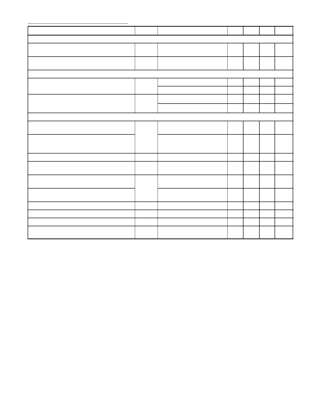
Electrical Characteristics (Cont’d): (VP = 8V, TA = +25°C, Note 2 unless otherwise specified)
Parameter
Symbol
Test Conditions
Min Typ Max Unit
Frequency Response at Voltage Outputs
Gain Decreases by Frequency Response at
Pin19, Pin16, Pin13
Gvf 70MHz
–
– –3 dB
Rise Time at Voltage Output
(Pin19, Pin16, Pin13)
trO 10% to 90% Amplitude,
Input Rise Time = 1ns
– 4.5 5.0 ns
Current Outputs (Pin20, Pin17, Pin14)
Signal Current (Black–to–White)
IO(b–w)
With Peaking, Note 7
– 50 – mA
–
– 100 mA
HF Saturation of Output Transistors
Threshold Voltages (Note 8)
V20–19,
17–16,
14.13
IO = 50mA
IO = 100mA
–
– 2.0 V
–
– 2.2 V
Threshold for Horizontal Blanking
V9
(Blanking, Output Clamping)
1.2 1.4 1.6 V
Threshold for Switch–Off
(Blanking, Minimum Black Level, No
Output Clamping)
5.8 6.5 6.8 V
Input Resistance Referenced to GND
Rg
Delay Between Horizontal Blanking Input
td9
and Output Signal Blanking
50 80 110 kΩ
– 35 60 ns
Threshold for Vertical Blanking
V10
(Blanking, No Input Clamping)
1.2 3.0 3.5 V
Threshold for Clamping
(Input Clamping, No Blanking)
2.6 3.0 3.5 V
Input Current
Rise and Fall Time for Clamping Pulse
Clamping Pulse Width
Delay Between Vertical Blanking Input
and Output Signal Blanking
I10
tr, f10
tw10
td10
Transition 1 to 3.5V
V10 = 3V
–3 –1 – µA
–
– 75 ns/V
0.6 – – µs
– 300 – ns
Note 2. All voltages measured to GND (Pin4).
Note 7. The external RC combination at Pin19, Pin16 and Pin13 enables peak currents during transients.
Note 8. The internal threshold voltages are derived from an internally stabilized voltage. The internal
pulses are generated if the input pulses are higher than the thresholds.
Share Link: 