NJU3504 データシートの表示(PDF) - Japan Radio Corporation
部品番号
コンポーネント説明
一致するリスト
NJU3504 Datasheet PDF : 60 Pages
| |||
NJU3504
*2 Memory Bank Register(PHY15) selects the Bank0 in ROM when LSB of PHY15 is written “0”, and
selects the Bank1 when LSB of PHY15 is written “1”.
The Bank0 is selected on “RESET” operation.
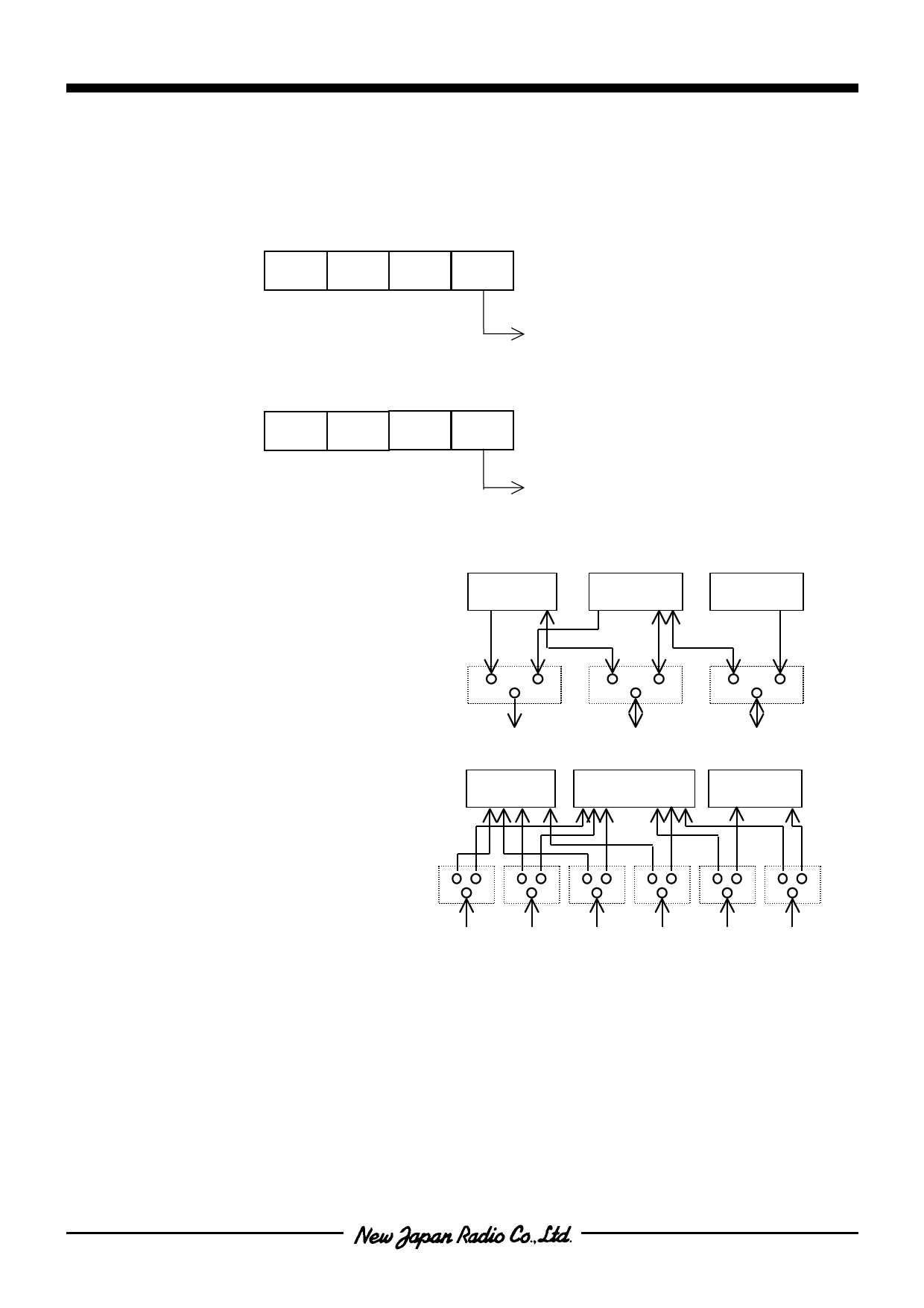
[Reading from the Memory Bank Register (PHY15)]
(MSB) 3
2
1
0 (LSB)
PHY15
“0”
“0”
“0”
[Writing to Memory Bank Register (PHY15)]
(MSB) 3
2
1
PHY15
−
−
−
Bank of ROM
/ 0:bank0, 1:bank1
0 (LSB)
Bank of ROM
/ 0:bank0, 1:bank1
Note) Bank0 Address : 000H − 7FFH, Bank1 Address : 800H − FFFH
*3 Wiring of terminals
The mask option selects a terminal
type from SDO/PL0, SDI(O)/PL1 or
SCK/CKOUT as shown in right.
PHY28
PHY2
Prescaler
*4 Wiring of terminals
The mask option selects a terminal
type from AIN0/PI0, AIN1/PI1,
AIN2/PI2, AIN3/PI3, VREF/PJ0, or
ADCK/PJ1 as shown in right.
SDO / PL0
PHY25
SDI(O) / PL1 SCK / CKOUT
ADC
PHY26
AIN0/PI0 AIN1/PI1 AIN2/PI2 AIN3/PI3 VREF/PJ0 ADCK/PJ1
- 13 -
Share Link: 