NJM2527 データシートの表示(PDF) - Japan Radio Corporation
部品番号
コンポーネント説明
一致するリスト
NJM2527 Datasheet PDF : 34 Pages
| |||
NJM2527
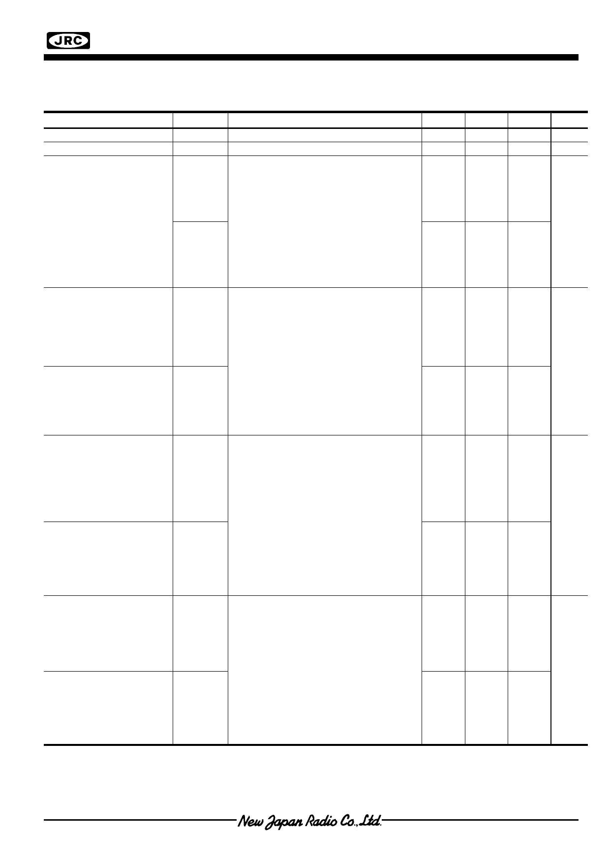
s ELECTRICAL CHARACTERISTICS
(Ta=25°C,VCC1=5V, VCC2=5V,TP20=TP31=TP45=2.5V,
TP19=2.8V,TP7=5V,TP38=1V,TP39=3V,TP44=0V,SW13=SW7=L)
PARAMETER
SYMBOL
TEST CONDITION (TP=IC Pin No.)
Operating Current 1
Operating Current 2
Contrast Adjust Gain
Variable Range
ICC1
ICC2
GCT1
GCT2
VCC1, No signal
VCC2, No signal
SG1 applied to TP33, TP35 and TP37.
SG10 applied to TP5, SG11 applied to
TP9, SG2 applied to TP11, define the
each amplitude (BLK-WHT) at
SW7=H, and TP31=0V, 2.5V,
5V as V1, V2 and V3.
Then measure the each output of the
non-inverting
GCT1=20LOG(V1/V2)
GCT2=20LOG(V3/V2)
Measure points are Rout, Gout, Bout.
Image Quality Adjust
Variable Minimum
Range (Y/C)
Image Quality Adjust
Variable Maximum
Range (Y/C)
Image Quality Adjust
Variable Minimum
Range (Composite)
Image Quality Adjust
Variable Maximum
Range (Composite)
Trap attenuation
(NTSC)
Trap attenuation
(PAL)
GPSMIN1
GPSMAX1
GPSMIN2
GPSMAX2
GCF NT
GCF PAL
SG3 (100KHz, 2.0MHz / 70mVp-p)
applied to TP28, SG10 applied to TP5,
SG11 applied to TP9, SG2 applied to
TP11, 1.5V applied to TP38, 3.2V
applied to TP39.measure amplitude on
TP2 of non-inverting. The each gain on
SG3 of sin signal of frequency define as
G(2.0M),G(100K).
GPSMIN1=G (2.0M)-G (100K)
At SW27=H, TP27=0V
GPSMAX1=G (2.0M)-G (100K)
At SW27=H, TP27=5V
SW13=H, TP13(B)=0V,
SG3 (100KHz, 2.0MHz / 70mVp-p)
applied to TP28, SG10 applied to TP5,
SG11 applied to TP9,SG2 applied to
TP11, 1.5V applied to TP38, 3.2V
applied to TP39.measure amplitude on
TP2 of non-inverting.The each gain on
SG3 of sin signal of frequency define as
G(2.0M),G (100K). (typical swing)
GPSMIN2=G (2.0M)-G (100K)
at SW27=H,TP27=0V
GPSMAX1=G (2.0M)-G (100K)
at SW27=H,TP27=5V
SW13=H, TP13(B)=0V,TP27=2.5V,SG2
applied to TP11, SG11 applied to TP9,
SG3 (100KHz, 3.579545MHz ,
4.43361875MHz 200mVpp) applied to
TP28.
B1, B2 define output swing of TP2
at TP19=2.8V,SG3 (3.579545MHz),
SG3 (100KHz). B3, B4 define output
swing of TP2 at TP19=0V, SG3
(4.43361875MHz), SG3 (100kHz).
GCFNT=20*LOG (B1/B2)
GCFPAL=20*LOG (B3/B4)
MIN.
-
-
-
1.0
-
10.0
-
6.0
-
-
TYP.
45.0
14.5
-12.0
2.5
0.0
15.0
-5.0
10.0
-45
-45
MAX.
60.0
20.0
UNIT
mA
mA
-9.0
dB
-
4.0
dB
-
-1.0
dB
-
-30
dB
-30
Ver.3
-3-
Share Link: 