NCV8675(2007) データシートの表示(PDF) - ON Semiconductor
部品番号
コンポーネント説明
一致するリスト
NCV8675
(Rev.:2007)
(Rev.:2007)
ON Semiconductor

NCV8675 Datasheet PDF : 15 Pages
| |||
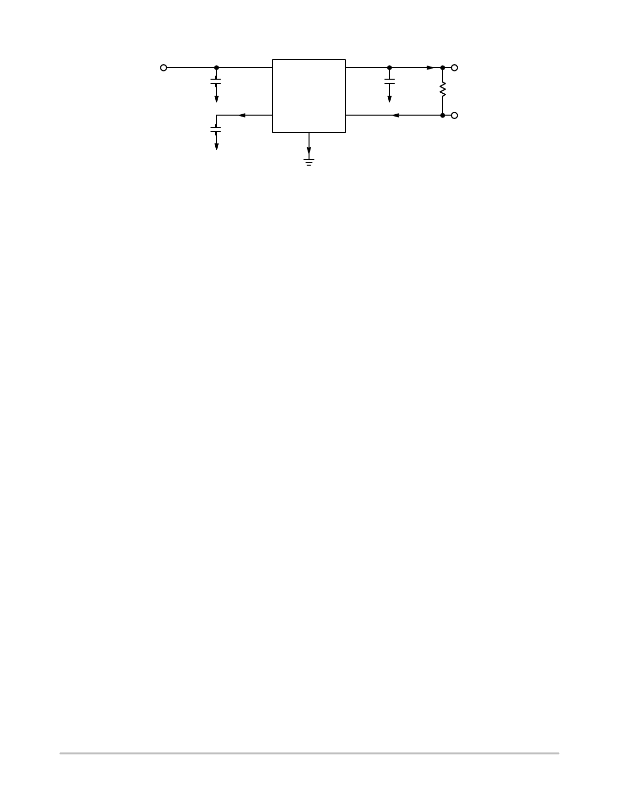
NCV8675
VIN
CIN
100 nF
IN
1
OUT
5
NCV8675
IOUT
COUT
22 mF
VOUT
REXT
5.0 K
ID D
RO
4
2
CD
3
IRO
VRO
47 nF
GND
IG
Figure 34. Application Circuits
Circuit Description
The NCV8675 is an integrated low dropout regulator that
provides 5.0 V 350 mA, or 3.3 V 350 mA protected output
and a signal for power on reset. The regulation is provided
by a PNP pass transistor controlled by an error amplifier
with a bandgap reference, which gives it the lowest possible
drop out voltage and best possible temperature stability. The
output current capability is 350 mA, and the base drive
quiescent current is controlled to prevent over saturation
when the input voltage is low or when the output is
overloaded. The regulator is protected by both current limit
and thermal shutdown. Thermal shutdown occurs above
150°C to protect the IC during overloads and extreme
ambient temperatures. The delay time for the reset output is
adjustable by selection of the timing capacitor. See
Figure 34, Test Circuit, for circuit element nomenclature
illustration.
Regulator
The error amplifier compares the reference voltage to a
sample of the output voltage (VOUT) and drives the base of
a PNP series pass transistor by a buffer. The reference is a
bandgap design to give it a temperature-stable output.
Saturation control of the PNP is a function of the load current
and input voltage. Oversaturation of the output power
device is prevented, and quiescent current in the ground pin
is minimized.
Regulator Stability Considerations
The input capacitor (CIN) is necessary to stabilize the
input impedance to avoid voltage line influences. The output
capacitor helps determine three main characteristics of a
linear regulator: startup delay, load transient response and
loop stability. The capacitor value and type should be based
on cost, availability, size and temperature constraints.
Ceramic, tantalum, or electrolytic capacitors of 22 mF, or
greater, are stable with very low ESR values. Refer to
Figure 2 for specific ESR ratings. The aluminum
electrolytic capacitor is the least expensive solution, but, if
the circuit operates at low temperatures (-25°C to -40°C),
both the capacitance and ESR of the capacitor will vary
considerably. The capacitor manufacturer's data sheet
usually provides this information. The value for the output
capacitor COUT shown in Figure 13, Test Circuit, should
work for most applications; however, it is not necessarily the
optimized solution.
Reset Output
The reset output is used as the power on indicator to the
microcontroller. This signal indicates when the output
voltage is suitable for reliable operation of the controller. It
pulls low when the output is not considered to be ready. RO
is pulled up to VOUT by an external resistor, typically 5.0 kW
in value. The input and output conditions that control the
Reset Output and the relative timing are illustrated in
Figure 35, Reset Timing. Output voltage regulation must be
maintained for the delay time before the reset output signals
a valid condition. The delay for the reset output is defined as
the amount of time it takes the timing capacitor on the delay
pin to charge from a residual voltage of 0 V to the upper
timing threshold voltage VDU of 1.3 V. The charging current
for this is ID of 4 mA. By using typical IC parameters with
a 47 nF capacitor on the D Pin, the following time delay is
derived:
tRD + CD * VDUńID
tRD + 47ĂnF * (1.3ĂV)ń4ĂmA + 15.3Ăms
Other time delays can be obtained by changing the CD
capacitor value. The Delay Time can be reduced by
decreasing the capacitance of CD. Using the formula above,
Delay can be reduced as desired. Leaving the Delay Pin
open is not desirable as it can result in unwanted signals
being coupled onto the pin.
http://onsemi.com
10
Share Link: