NCV8660 データシートの表示(PDF) - ON Semiconductor
部品番号
コンポーネント説明
一致するリスト
NCV8660 Datasheet PDF : 14 Pages
| |||
NCV8660
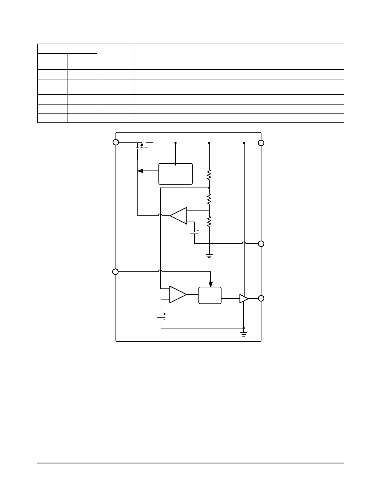
PIN DESCRIPTIONS
Pin
DPAK
SOIC−8
FUSED
1
1
2
2
3, Tab
5−8
4
3
5
4
Symbol
IN
RO
GND
DT
OUT
Function
Input Supply Voltage. 0.1 mF bypass capacitor to GND at the IC.
Reset Output. CMOS compatible output. Goes low when VOUT drops by more than 7%
from nominal.
Ground
Reset Delay Time Select. Short to GND or connect to OUT to select time.
Regulated Voltage Output. 2.2 mF to ground for typical applications.
IN
OUT
Current Limit
and Thermal
Shutdown
+
−
Vref1
GND
DT
−
Timing
+
Circuit
RO
Vref2
Figure 2. Block Diagram
http://onsemi.com
2
Share Link: 