NCV4269 データシートの表示(PDF) - ON Semiconductor
部品番号
コンポーネント説明
一致するリスト
NCV4269
ON Semiconductor

NCV4269 Datasheet PDF : 16 Pages
| |||
NCV4269
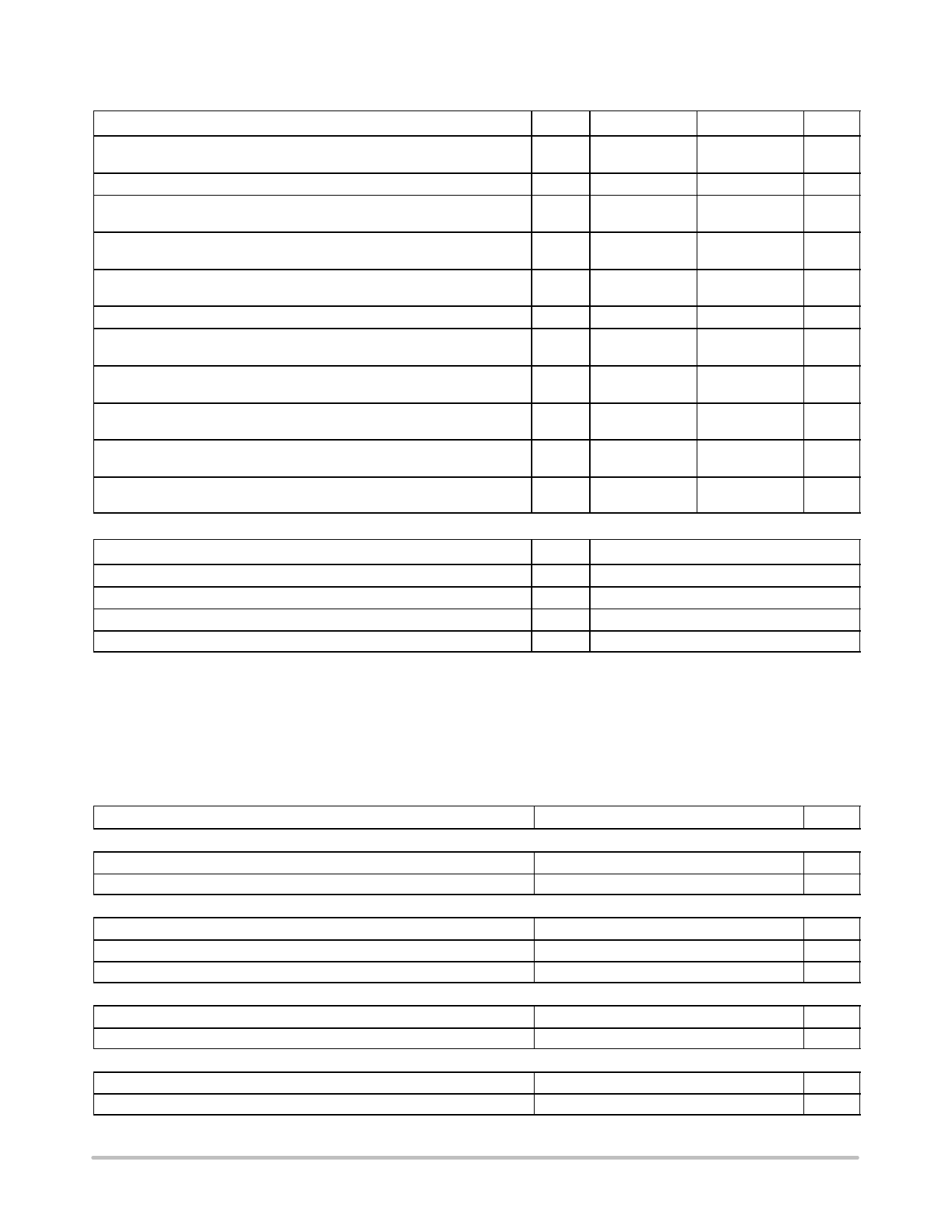
MAXIMUM RATINGS (TJ = −40°C to 150°C)
Parameter
Symbol
Min
Max
Unit
Input to Regulator
Input Transient to Regulator
Sense Input
Reset Threshold Adjust
Reset Delay
Ground
Reset Output
Sense Output
Regulated Output
Junction Temperature
Storage Temperature
Input Voltage Operating Range
Junction Temperature Operating Range
Lead Temperature Soldering and MSL
VI
−40
45
V
II
Internally Limited Internally Limited
VI
−
60
V
VSI
−40
ISI
−1
45
V
1
mA
VRADJ
IRADJ
−0.3
−10
7
V
10
mA
VD
−0.3
7
V
ID Internally Limited Internally Limited
Iq
50
−
mA
VRO
−0.3
7
V
IRO Internally Limited Internally Limited
VSO
−0.3
7
V
ISO Internally Limited Internally Limited
VQ
−0.5
IQ
−10
7.0
V
−
mA
TJ
−
TSTG
−50
150
°C
150
°C
VI
−
TJ
−40
45
V
150
°C
Parameter
Symbol
Value
MSL, 20−Lead LS Temperature 265°C Peak (Note 3)
MSL
3
MSL, 20−Lead, LS Temperature 240°C Peak (Note 4)
MSL
1
MSL, 8−Lead, 14−Lead, LS Temperature 265°C Peak (Note 3)
MSL
1
MSL, 8−Lead EP, LS Temperature 260°C
MSL
2
Stresses exceeding Maximum Ratings may damage the device. Maximum Ratings are stress ratings only. Functional operation above the
Recommended Operating Conditions is not implied. Extended exposure to stresses above the Recommended Operating Conditions may affect
device reliability.
1. This device series incorporates ESD protection and exceeds the following ratings:
Human Body Model (HBM) ≤ 2.0 kV per JEDEC standard: JESD22–A114.
Machine Model (MM) ≤ 200 V per JEDEC standard: JESD22–A115.
2. Latchup Current Maximum Rating: ≤ 150 mA per JEDEC standard: JESD78.
3. +5°C/−0°C, 40 Sec Max−at−Peak, 60 − 150 Sec above 217°C.
4. +5°C/−0°C, 30 Sec Max−at−Peak, 60 − 150 Sec above 183°C.
THERMAL CHARACTERISTICS
Characteristic
Test Conditions (Typical Values)
Unit
SO−8 Package (Note 5)
Junction−to−Pin 4 ( Y − JL4, YL4)
Junction−to−Ambient Thermal Resistance (RqJA, qJA)
SO−8 EP Package (Note 5)
Junction−to−Pin 8 ( Y − JL8, YL8)
Junction−to−Ambient Thermal Resistance (RqJA, qJA)
Junction−to−Pad ( Y − JPad)
SO−14 Package (Note 5)
Junction−to−Pin 4 ( Y − JL4, YL4)
Junction−to−Ambient Thermal Resistance (RqJA, qJA)
SO−20 Package (Note 5)
Junction−to−Pin 4 ( Y − JL4, YL4)
Junction−to−Ambient Thermal Resistance (RqJA, qJA)
5. 2 oz copper, 50 mm2 copper area, 1.5 mm thick FR4
53.8
170.9
23.7
71.4
7.7
18.4
111.6
21.8
95.3
°C/W
°C/W
°C/W
°C/W
°C/W
°C/W
°C/W
°C/W
°C/W
http://onsemi.com
3
Share Link: