NCP1398CDR2G データシートの表示(PDF) - ON Semiconductor
部品番号
コンポーネント説明
一致するリスト
NCP1398CDR2G
ON Semiconductor

NCP1398CDR2G Datasheet PDF : 24 Pages
| |||
NCP1398B/C
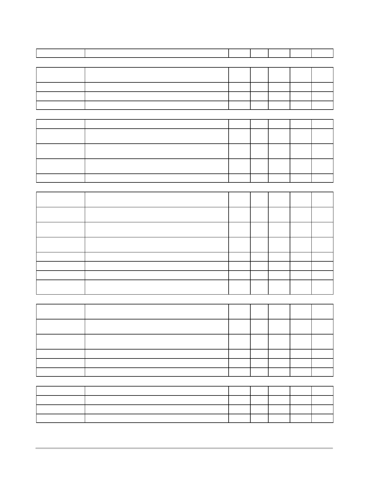
ELECTRICAL CHARACTERISTICS
(For typical values TJ = 25°C, for min/max values TJ = −40°C to +125°C, Max TJ = 150°C, VCC = 12 V unless otherwise noted)
Symbol
Rating
Pin
Min Typ
Max
Unit
VOLTAGE CONTROL OSCILLATOR (VCO)
Fsw_max
Maximum switching frequency clamp, Rfmax = 7.2 kW on pin 4,
Vpin 7 ramps up above 5.3 V, DT = 300 ns
4
465 525
585
kHz
DC
Operating duty−cycle symmetry
10−14 48
50
52
%
Tdel
Delay before driver re−start from fault, skip or disable mode
−
−
10
−
ms
Vref_Rt
Reference voltage for Rt pin
5
2.18 2.3
2.42
V
FEEDBACK SECTION
Rfb
Internal pull−down resistor
7
−
20
−
kW
Vfb_min
Voltage on pin 7 below which the VCO has no action and Fmin
7
−
1.1
−
V
clamp is reached
Vfb_max
Voltage on pin 7 below which the VCO has no action and Fmax
7
−
5.5
−
V
clamp is reached
Vfb_fault
Voltage on pin 7 below which the controller considers the FB fault 7
240 280
320
mV
(Note 4)
Vfb_fault_hyste Feedback fault comparator hysteresis (Note 4)
7
−
45
−
mV
DRIVE OUTPUT AND DEAD−TIME CLAMP
Tr
Output voltage rise−time @ CL = 1 nF, 10−90% of output signal 14−15/ −
40
−
ns
12−11
Tf
Output voltage fall−time @ CL = 1 nF, 10−90% of output signal 14−15/ −
20
−
ns
12−11
ROH
Source resistance
14−15/ −
13
−
W
12−11
ROL
Sink resistance
14−15/ −
5.5
−
W
12−11
T_dead_nom
T_dead_max
T_dead_min
IHV_LEAK
Dead time with RDT = 10 kW from pin 6 to GND
Maximum dead−time with RDT = 71.5 kW from pin 6 to GND
Minimum dead−time, RDT = 2.8 kW from pin 6 to GND
Leakage current on high voltage pins to GND
6
250 290
340
ns
6
−
1.9
−
ms
6
−
100
−
ns
14, 15, −
−
16
5
mA
FAULT TIMER
Itimer
Timer capacitor charge current during feedback fault or when
Vref_fault < Vpin9 < Vref_OCP
3
165 195
215
mA
T−timer
Timer duration with a 1 mF capacitor and a 1 MW resistor, Itimer1
3
−
19.3
−
ms
current applied (Note 3)
T−timerR
Timer recurrence in permanent fault, same values as above
(Note 3)
3
−
1.4
−
s
VtimerON
Voltage at which pin 3 stops output pulses
3
3.8
4
4.2
V
VtimerOFF
Voltage at which pin 3 re−starts output pulses
3
0.95
1
1.05
V
Rtimer_dis
Timer discharge switch resistance (Note 3)
1
−
100
−
W
BROW−OUT PROTECTION
IBO_bias
Brown−Out input bias current (Note 3)
1
−
−
0.01
mA
VBO
Brown−Out level
1
0.98 1.008 1.08
V
VBO_hyst
Brown−Out comparator hysterisis
1
−
10
−
mV
Tfl_BO
BO filter duration (Note 3)
1
−
20
−
ms
3. Guaranteed by design.
4. Not tested for NCP1398C.
http://onsemi.com
6
Share Link: