NCP1397A データシートの表示(PDF) - ON Semiconductor
部品番号
コンポーネント説明
一致するリスト
NCP1397A
ON Semiconductor

NCP1397A Datasheet PDF : 27 Pages
| |||
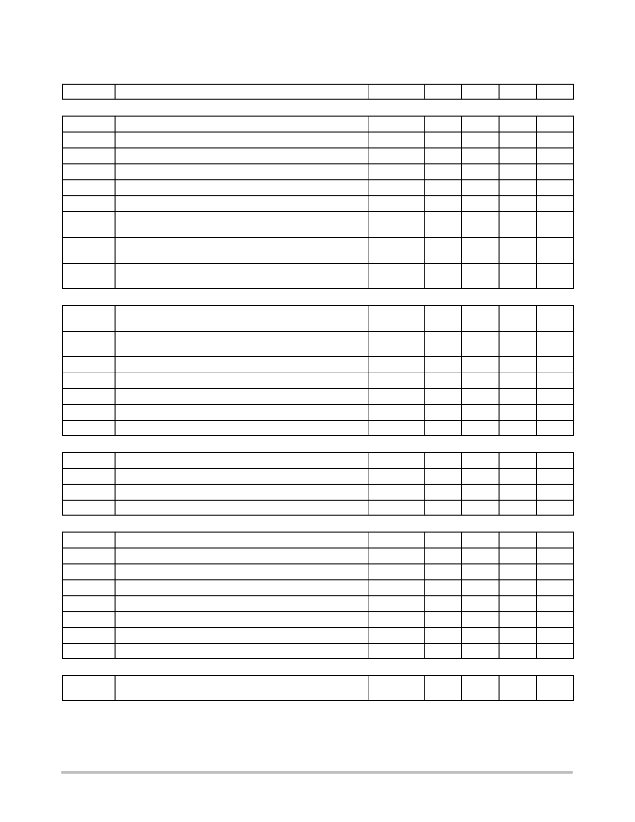
NCP1397A, NCP1397B
ELECTRICAL CHARACTERISTICS (For typical values TJ = 25°C, for min/max values TJ = −40°C to +125°C, Max TJ = 150°C, VCC
= 12 V unless otherwise noted)
Symbol
Rating
Pin
Min
Typ
Max Unit
SUPPLY SECTION
VCC(on) Turn−on threshold level, VCC going up
VCC(min) Minimum operating voltage after turn−on
Vboot(on) Startup voltage on the floating section
Vboot(min) Cutoff voltage on the floating section
Istartup
Startup current, VCC < VCC(on)
VCC(reset) VCC level at which the internal logic gets reset
ICC1
Internal IC consumption, no output load on pin 15/14 – 11/10,
FSW = 300 kHz
ICC2
Internal IC consumption, 1 nF output load on pin 15/14 – 11/10,
FSW = 300 kHz
ICC3
Consumption in fault or disable mode (All drivers disabled,
Rt = 34 kW, RDT = 10 kW)
VOLTAGE CONTROL OSCILLATOR (VCO)
12
12
16−14
16−14
12
12
12
12
12
9.7
10.5 11.3
V
8.7
9.5
10.3
V
8
9
10
V
7.4
8.4
9.4
V
−
−
300
mA
−
6.6
−
V
−
4
−
mA
−
11
−
mA
−
1.5
−
mA
FSW(min) Minimum switching frequency, Rt = 34 kW on pin 4, Vpin6 = 0.8 V,
DT = 300 ns
4
58.2
60
61.8
kHz
FSW(max) Maximum switching frequency, Rf(max) = 1.9 kW on pin 2, Vpin6 >
5.3 V, Rt = 34 kW, DT = 300 ns
2
440
500
560
kHz
FBSW
DC
Feedback pin swing above which Df = 0
Operating duty−cycle symmetry
6
−
5.3
−
V
11−15
48
50
52
%
Tdel1
Delay before driver restart from fault or disable mode
Tdel2
Delay before driver restart after VCC(on) event (Note 4)
Vref(Rt) Reference voltage for Rt pin
FEEDBACK SECTION
−
−
700
−
ns
−
−
11
−
ms
4
2.18
2.3
2.42
V
RFB
Internal pulldown resistor
6
−
20
−
kW
VFB(min) Voltage on pin 6 below which the FB level has no VCO action
6
−
1.1
−
V
VFB(off) Voltage on pin 6 below which the controller considers the FB fault
6
240
280
320
mV
VFBoff(hyste) Feedback fault comparator hysteresis
6
−
45
−
mV
DRIVE OUTPUT
Tr
Tf
ROH
ROL
Tdead
Tdead(max)
Tdead(min)
IHV(LEAK)
TIMERS
Output voltage risetime @ CL = 1 nF, 10−90% of output signal
Output voltage falltime @ CL = 1 nF, 10−90% of output signal
Source resistance
Sink resistance
Deadtime with RDT = 10 kW from pin 7 to GND
Maximum deadtime with RDT = 82 kW from pin 7 to GND
Minimum deadtime, RDT = 3 kW from pin 7 to GND
Leakage current on high voltage pins to GND
15−14/11−10 −
40
−
ns
15−14/11−10 −
20
−
ns
15−14/11−10 −
13
−
W
15−14/11−10 −
5.5
−
W
7
250
290
340
ns
7
−
2
−
ms
7
−
100
−
ns
14, 15,16
−
−
5
mA
Itimer1
Timer capacitor charge current during feedback fault or when
Vref(fault) < Vpin9 < Vref(OCP)
3
150
175
190
mA
3. The IC does not activate soft−start (unless the feedback pin voltage is below 0.3 V) when the skip/disable input is released, this is for skip
cycle implementation.
4. Guaranteed by design.
http://onsemi.com
6
Share Link: