MT9162 データシートの表示(PDF) - Mitel Networks
部品番号
コンポーネント説明
一致するリスト
MT9162 Datasheet PDF : 17 Pages
| |||
MT9162
Advance Information
VBias 1
VRef 2
PWRST 3
IC 4
A/µ 5
RXMUTE 6
TXMUTE 7
CSL0 8
CSL1 9
CSL2 10
20 AIN+
19 AIN-
18 VSS
17 AOUT +
16 AOUT -
15 VDD
14 CLOCKin
13 STB
12 Din
11 Dout
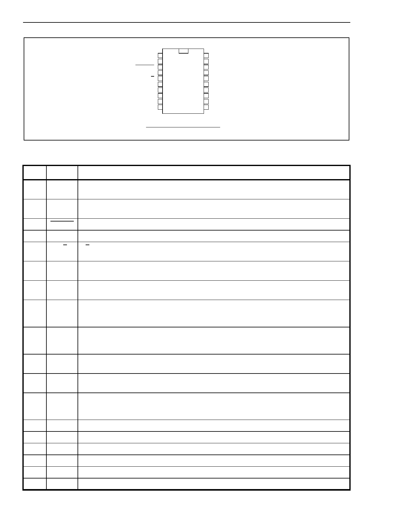
20 PIN PDIP/SOIC/SSOP
Pin Description
Figure 2 - Pin Connections
Pin # Name
Description
1
VBias Bias Voltage (Output). (VDD/2) volts is available at this pin for biasing external amplifiers.
Connect 0.1 µ F capacitor to VSS. Connect 1 µF capacitor to Vref.
2
VRef Reference Voltage for Codec (Output). Nominally [(VDD/2)-1.9] volts. Used internally.
Connect 0.1 µ F capacitor to VSS. Connect 1 µF capacitor to VBias
3 PWRST Power-up Reset. Resets internal state of device via Schmitt Trigger input (active low).
4
IC Internal Connection. Tie externally to VSS for normal operation.
5
A/µ A/µ Law Selection. CMOS level compatable input pin governs the companding law used by
the device. A-law selected when pin tied to VDD or µ-law selected when pin tied to VSS.
6 RXMute Receive Mute. When 1, the transmit PCM is forced to negative zero code. When 0, normal
operation. CMOS level compatible.
7 TXMute Transmit Mute. When 1, the transmit PCM is forced to negative zero code. When 0, normal
operation. CMOS level compatible.
8
CSL0 Clock Speed Select. These pins are used to program the speed of the SSI mode as well as
9
CSL1 the conversion rate between the externally supplied MCL clock and the 512 kHz clock required
10 CSL2 by the filter/codec. Refer to Table 2 for details. CMOS level compatible.
11
Dout Data Output. A tri-state digital output for 8-bit wide channel data being sent to the Layer 1
device. Data is shifted out via the pin concurrent with the rising edge of BCL during the timeslot
defined by STB.
12
Din Data Input. A digital input for 8-bit wide data from the layer 1 device. Data is sampled on the
falling edge of BCL during the timeslot defined by STB. CMOS level compatible.
13
STB Data Strobe. This input determines the 8-bit timeslot used by the device for both transmit and
receive data. This active high signal has a repetition rate of 8 kHz. CMOS level compatible.
14 CLOCKin Clock (Input). The clock provided to this input pin is used by the internal device functions.
Connect bit clock to this pin when it is 512 kHz or greater. Connect a 4096 kHz clock to this pin
when the bit clock is 128 kHz or 256 kHz. CMOS level compatible.
15
VDD Positive Power Supply. Nominally 5 volts.
16 AOUT- Inverting Analog Output. (balanced).
17 AOUT+ Non-Inverting Analog Output. (balanced).
18
VSS Ground. Nominally 0 volts.
19
Ain- Inverting Analog Input. No external anti-aliasing is required.
20
Ain+ Non-Inverting Analog Input. Non-inverting input. No external anti-aliasing is required.
7-162
Share Link: 