MSM7715 データシートの表示(PDF) - Oki Electric Industry
部品番号
コンポーネント説明
一致するリスト
MSM7715 Datasheet PDF : 21 Pages
| |||
¡ Semiconductor
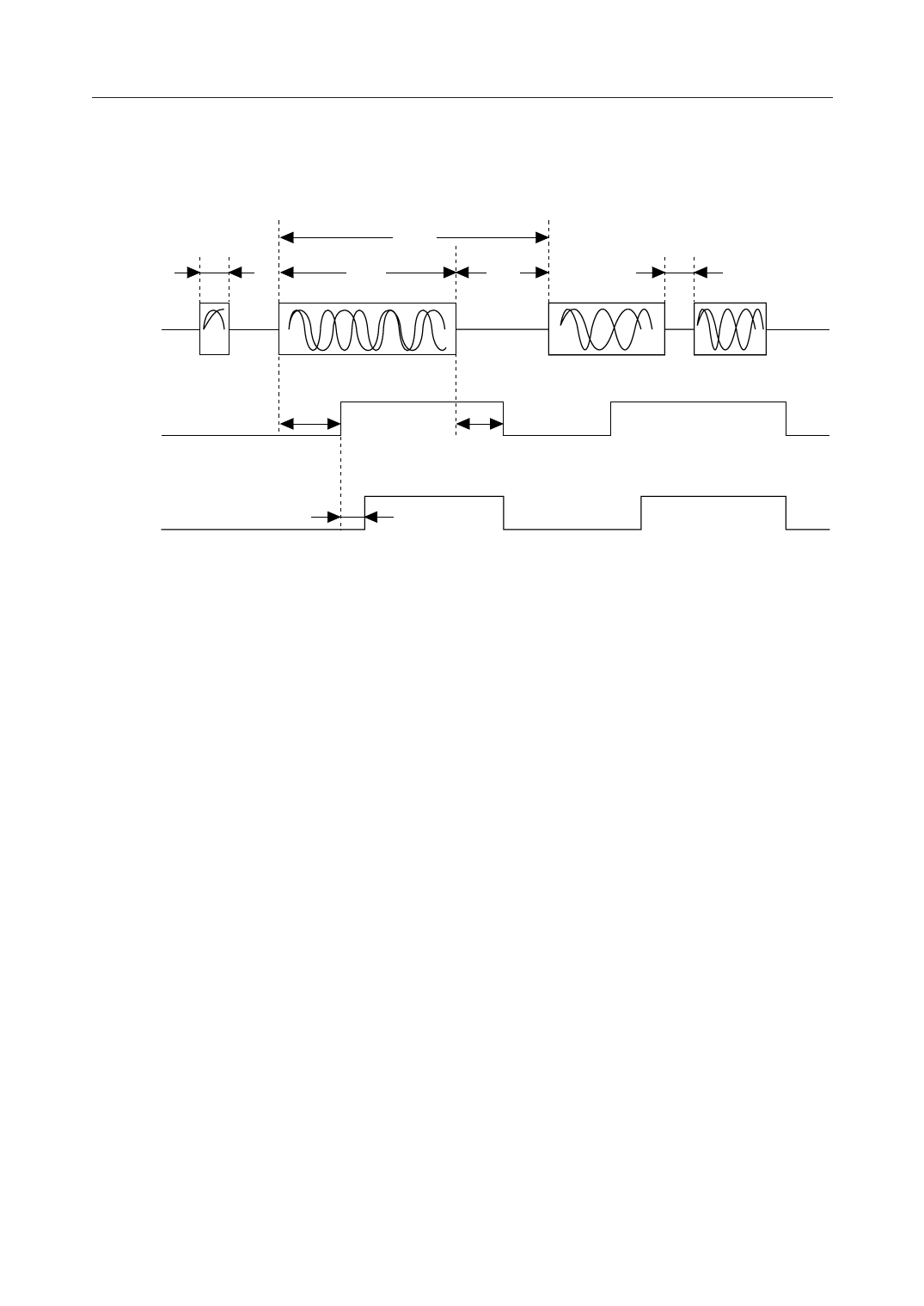
TIMING DIAGRAM
When DTMF is received
tC
tI
tS
tP
AIN signal
tG
DT1 to 4
tD
MSM7715
tB
SP
tSP
Figure 1 DTMF Receive Timing
tS
: Tone time for detect
When the input signal duration is tS or more, receiving is normally done.
tI
: Tone time for no detect
When the input signal duration is tI or less, this input signal is ignored and DT1 to
DT4 and SP is not output.
tP
: Interdigit pause time
When there is no input signal for tP or more, DT1 to DT4 and SP are reset.
tB
: Acceptable drop out time
DT1 to DT4 and SP are not reset even though a no-signal state for tB or less
(momentary no-signal) occurs during signal receiving. The tB is applicable while
the received signals are output. (SP="1")
tSP
: SP delay time
Against the DT1 to DT4 output, SP is output after a delay of tSP. Therefore, latch DT1
to DT4 at the rising edge of SP.
tC
: Signal repetition time
For normal receiving, set the signal repetition time to tC or more.
tG1n
: Output delay time (n: 1 or 2)
Against the appearance of the input signal, DT1 to DT4 are outputs after a delay of
tG1n.
tD
: Output trailing edge delay time
Against the stop of the input signal, DT1 to DT4 and SP stop outputting after a delay
of tD.
10/21
Share Link: 