MRFIC1504R2 データシートの表示(PDF) - Motorola => Freescale
部品番号
コンポーネント説明
一致するリスト
MRFIC1504R2 Datasheet PDF : 8 Pages
| |||
ARCHIVED BY FREESCALE SEMICOFNrDeUeCsTOcRa, IlNeC.S2M0eR0m5FICic1o50n4ductor, Inc.
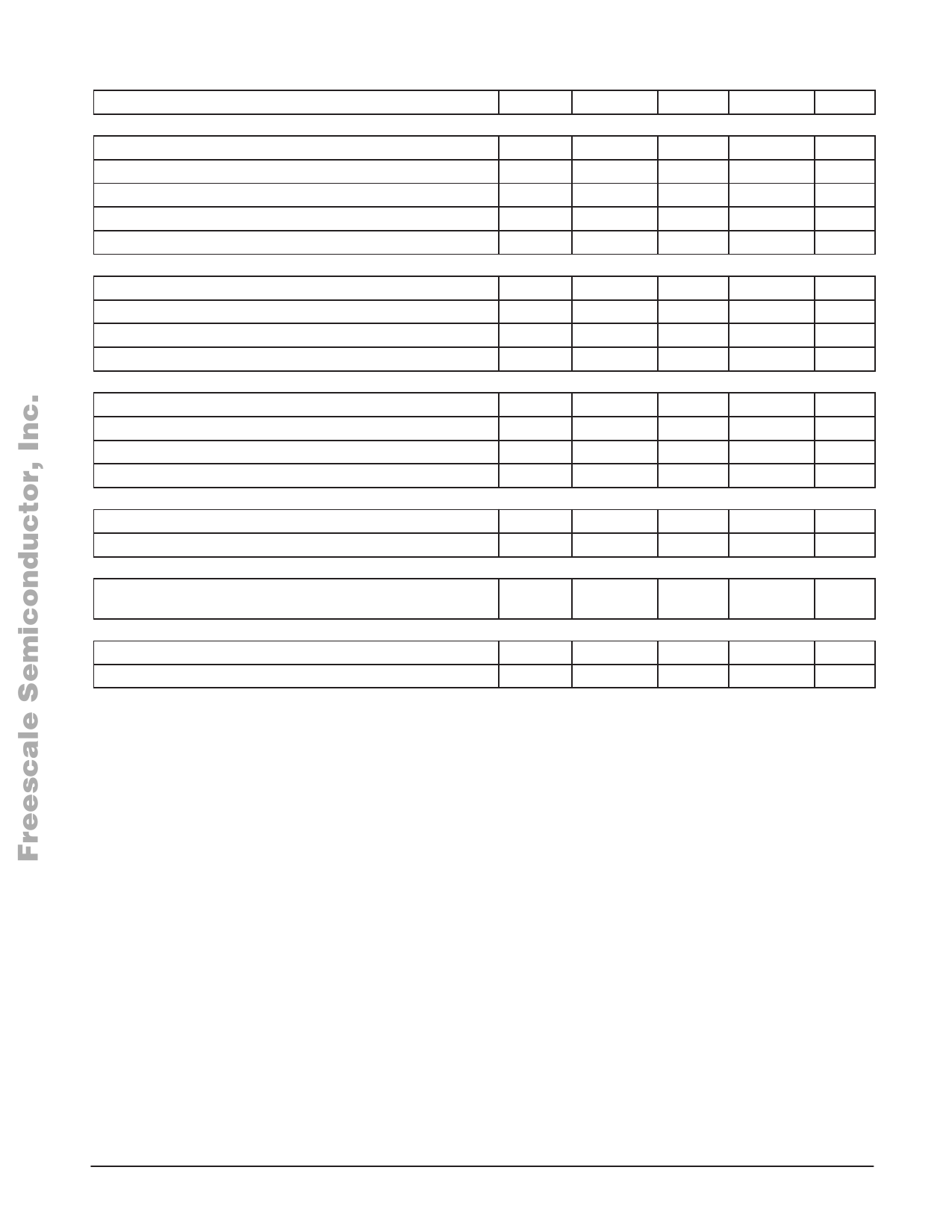
ELECTRICAL CHARACTERISTICS — continued (VCC = 2.7 to 3.3 V; TA = –40 to 85°C; Enable = 2.7 V unless otherwise noted)
Characteristic
Symbol
Min
Typ
Max
Unit
LIMITING AMPLIFIER
Second Intermediate Frequency
Input Signal Level
ø Output Voltage Swing (Into 10 pf 100 kΩ)
DC Output Level
fIF2
–
Vout
–
–
4.092
4.0
11
800
–
–
1.4
–
MHz
31
mV
–
mVpp
–
V
Gain
G
–
50
–
dB
REFERENCE OSCILLATOR
Reference Frequency
Reference Frequency Input Level (Crystal Output Pin)
fr
–
16.368
–
MHz
–
–
500
–
mVpp
Reference Oscillator Output Voltage Level (Into 15 pF || 10 kΩ)
–
750
–
–
mVpp
Reference Clock Input Drive Level
–
400
800
1500
mVpp
PLL
First Local Oscillator Frequency
Second Local Oscillator Frequency
VCO C/N (at 10 kHz Offset)
fLO1
fLO2
–
–
1636.8
–
MHz
–
65.47
–
MHz
–
–80
–
dBc/Hz
VCO Gain (TBD Varactor)
–
–
20
–
MHz/V
ENABLE
Enable Active Level
Disable Active Level
VOLTAGE REGULATOR
–
0.8 VCC
VCC
–
V
–
–
0
0.2 VCC
V
Regulator Output Voltage
(VCC = 2.7 to 3.3 V, Iout = 3.0 mA)
Vo
2.1
2.3
2.5
V
TEMPERATURE SENSE SPECS
Temperature Sensor Output Voltage @ 25°C
–
1.2
1.28
1.375
V
Temperature Sensor Slope over Temperature
–
–
5.0
–
mV/°C
MOTOROLA RF/IF DEVICE DATA For More Information On This Product,
3
Go to: www.freescale.com
Share Link: 