T15N1024A データシートの表示(PDF) - Taiwan Memory Technology
部品番号
コンポーネント説明
一致するリスト
T15N1024A Datasheet PDF : 13 Pages
| |||
tm TE
CH
TIMING WAVEFORMS
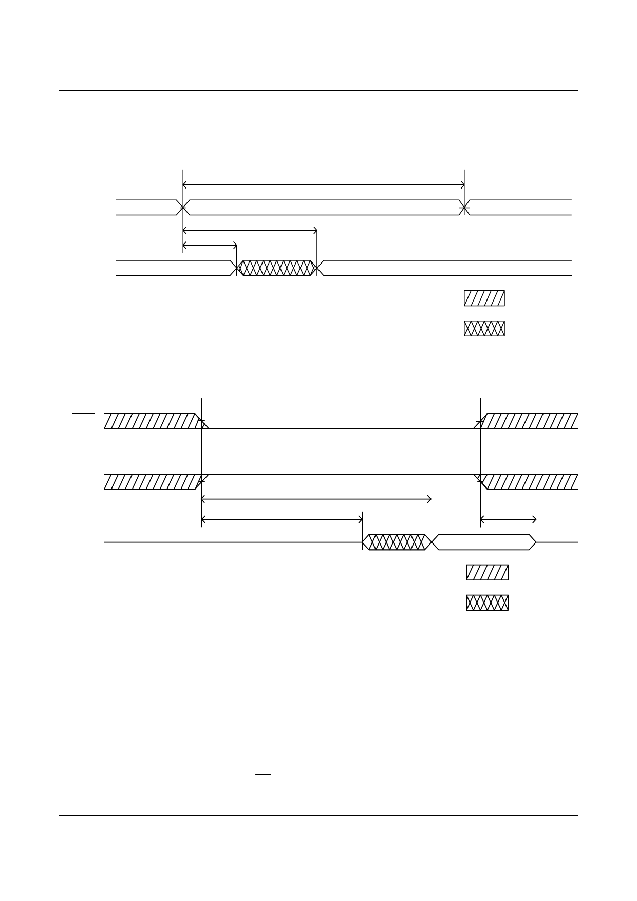
READ CYCLE 1
(Address Controlled)
tRC
Address
tAA
tOH
Dout Previous Data Vaild
Data Vaild
READ CYCLE 2
(Chip Enable Controlled)
CE1
T15N1024A
DON'T CARE
UNDEFINED
CE2
Dout
tACE
tLZ
tHZ
DON'T CARE
UNDEFINED
Notes (READ CYCLE) :
1. WE are high for read cycle.
2. All read cycle timing is referenced from the last valid address to the first transition address.
3. tHZ and tOHZ are defined as the time at which the outputs achieve the open circuit condition referenced to
VOH or VOL levels.
4. At any given temperature and voltage condition. tHZ (max.) is less than tLZ (min.) both for a given device
and from device to device interconnection.
5. Transition is measured ±200mV from steady state voltage with load. This parameter is sampled and not
100% tested.
6. Device is continuously selected with CE1 =VIL .
TM Technology Inc. reserves the right
P. 7
to change products or specifications without notice.
Publication Date: FEB. 2003
Revision:E
Share Link: 